Silicon Wafer Laser Marking
Evaluate surface identification, wafer-edge marks and fine micro marks from the actual silicon, surface stack, side, thickness and damage limits—not from the word “wafer” alone. UV, green and near-infrared routes should be compared as sample-test hypotheses before a process or machine is released.
Silicon Can Be Marked, but the Approved Result Is Wafer-Specific
A laser can create a controlled surface change, a shallow ablated feature or remove a selected surface layer on some silicon wafers. Whether that result is acceptable depends on the wafer construction and what the next process must protect.
- Identify monocrystalline or polycrystalline silicon, supplier grade, type and known doping information where available.
- Record polished, ground, textured or otherwise prepared surfaces and every oxide, nitride, resist, passivation or coating layer in the mark area.
- Separate frontside, backside, bevel and edge locations because focus, contamination and fracture risk can change.
- Define visible contrast, code readability, permitted removal and damage limits before choosing a laser route.
- Approve the result after cleaning and inspection on production-representative wafers, not only on a convenient coupon.
No universal parameter table
Power, pulse width, frequency, scan speed, hatch, focus offset and pass count do not transfer safely from one wafer stack to another. A controlled test matrix is the defensible starting point.
Define the Wafer State Before Comparing Laser Sources
The base material name is only the first input. The mark interacts with the final surface presented to the beam.
Silicon identity
Record mono- or polycrystalline material, supplier designation, conductivity type, resistivity or doping information when it is relevant and available. Do not infer a process window from color alone.
Surface preparation
Identify polished, lapped, ground, textured, etched or otherwise prepared surfaces. Roughness and finish can change local absorption, contrast and particle behavior.
Layer stack
List native or grown oxide, nitride, passivation, resist, coating, metallization or temporary protection in the mark zone. Clarify whether the target is silicon or a layer above it.
Geometry
Provide diameter, thickness, bow or warp limits, edge profile, notch or flat, mark zone and nearby exclusion areas. Geometry affects support, focus and edge safety.
Process condition
State whether the wafer is bare, patterned, coated, diced or assembled, and whether marking occurs before or after sensitive cleaning, bonding, coating or device steps.
Acceptance boundary
Define the allowed optical change, removal, depth, particle level, edge damage, microcrack indication, cleanliness and functional checks. “Readable” alone is rarely enough.
Where Is Silicon Wafer Laser Marking Used, and Why?
Laser marking is commonly evaluated when a wafer needs durable identification or machine-readable traceability without adding ink, labels or a separate attached identifier. The exact location and mark method still have to fit the wafer surface and the next manufacturing step.
Wafer identification
Use a permanent ID to distinguish individual wafers, lots or process records where the identification must remain associated with the physical wafer.
Process traceability
Marking can support tracking through inspection, handling, cleaning, coating, bonding or other controlled process stages when the identification scheme and mark location are compatible with the workflow.
Automated reading
Machine-readable symbols or OCR-capable characters can support camera-based identification, but the code geometry, lighting, reader and surface response must be validated together.
Re-identification after processing
A durable mark may help preserve identity after selected processing steps, provided the mark survives the process and does not contaminate or interfere with the wafer surface.
Inspection and record matching
Readable wafer identification can help connect a physical wafer with inspection, metrology or production records when the data workflow is defined by the manufacturing system.
Location-specific identification
Frontside, backside and edge or bevel locations may serve different handling and traceability needs. The chosen position must stay outside protected areas and be tested as its own process condition.
What Is Usually Marked on a Silicon Wafer?
The useful question is not only whether the laser can make a visible mark, but whether it can reproduce the required identification format at the intended size and location with enough margin for the chosen inspection method.
Alphanumeric wafer ID
Serial references, wafer identifiers, lot-related characters or other controlled alphanumeric data may be marked for human, microscope or OCR-assisted reading.
Machine-readable 2D symbol
Compact 2D codes can be evaluated when automated identification is required. Cell size, quiet zone, local contrast, surface texture, illumination and reader setup all affect the usable margin.
Microtext or compact characters
Small text may be needed where the available mark zone is restricted. Specify minimum character height, stroke width, orientation and the actual inspection magnification or camera.
Do not choose the marking content independently from the wafer location
A code that is readable on a flat backside area may not transfer to a bevel or edge. Data format, mark size and location should be defined together with the wafer drawing, exclusion zones and inspection method.
Define the Result You Need Before Choosing the Marking Mechanism
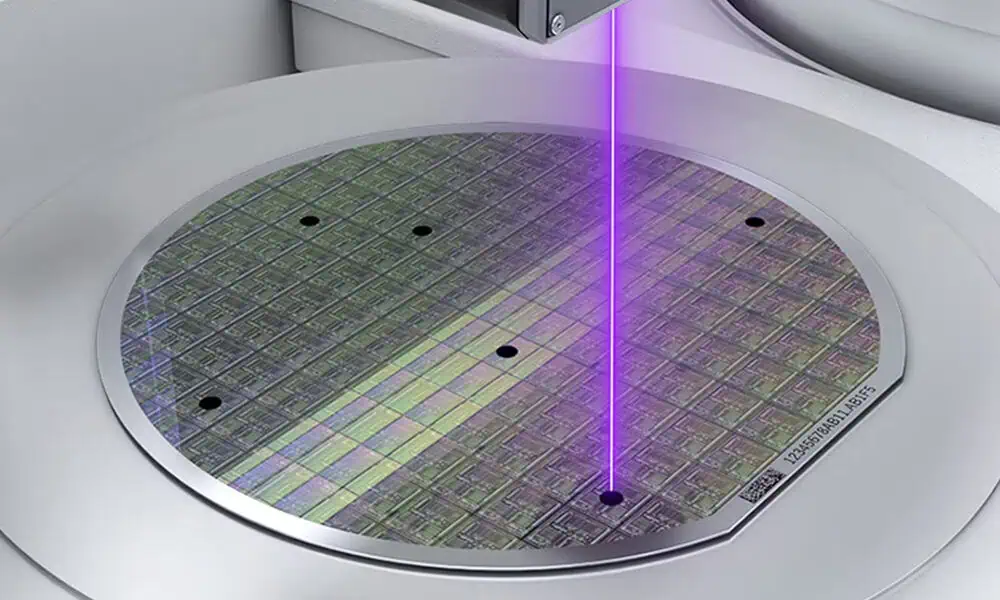
Start with the acceptance result: readable identification, controlled depth, low debris, limited surface change or selective layer removal. Then determine which physical marking mechanism can produce that result on the actual wafer stack.
Readable optical contrast
For visible or camera-readable identification, define the required contrast under the actual lighting and reader. The process may rely on a controlled optical or texture change, but readability must be released with the intended inspection system.
Low-damage surface mark
When removal must be limited, define the permitted texture change, particles, recast, microcrack indication and cleaning response. A mark that looks dark enough can still fail the damage boundary.
Shallow permanent geometry
If durability depends on physical relief, define the acceptable profile or depth and inspect recast, debris and local damage. Shallow micro-ablation can create durable geometry, but it requires tighter process-control evidence.
Selective layer removal
If the target is an oxide, passivation, resist, coating or metallized layer, define the layer to remove, the stop surface and the allowable exposure beneath it. This is a layer-selective process, not a universal silicon mark.
Human-readable microtext
Define minimum character height, stroke width, orientation and the microscope or camera used for acceptance. Nominal spot size alone does not prove reliable production text.
Machine-readable code
Define content, cell geometry, quiet zone, illumination, reader and grading or read criterion. Release the complete code-and-reader system rather than the appearance of one favorable sample.
Result first, mechanism second
Contrast change, fine roughening, shallow ablation and selective layer removal are different mechanisms. The correct mechanism is the one that meets the required readability or identification result while staying inside the wafer’s damage, contamination and downstream-process limits.
Frontside, Backside and Edge Marks Are Different Test Problems
Location changes the nearby layers, focus geometry, support method and downstream risk. Approve each intended mark location rather than assuming one result transfers around the wafer.
Protect active or patterned regions
Confirm the exact layer under the beam, exclusion zones, particle limits and whether any optical or thermal change can affect a later process. A cosmetic result does not establish device safety.
Check finish, chuck contact and later bonding
Backside roughness, films, thinning condition and support method can change mark response. Validate cleanliness, flatness and any interface used by downstream handling or bonding.
Control focus and brittle-edge loading
The curved edge presents a changing angle and working distance near a mechanically sensitive region. Fixture contact, mark depth, debris, chips and microcracks require explicit inspection.
How Do Diameter, Thickness, Bow, Warp and Edge Geometry Change the Process?
Wafer geometry changes how the part can be supported, how reliably the surface stays in focus and how much mechanical margin exists near the edge. These variables can change the fixture, focus strategy and inspection plan even when the silicon surface stack is unchanged.
Diameter
Larger or different wafer formats change the support area, handling method, reachable mark zone and fixture design. Confirm whether the mark must be reached in a fixed orientation or after notch/flat alignment.
Thickness
Thin or thinned wafers are more sensitive to support conditions, point loading and deflection. The fixture should hold the wafer without creating local stress or contaminating protected surfaces.
Bow and warp
Surface-height variation can move the mark plane away from nominal focus. Small features and codes may need tighter height control, a restricted mark zone or an autofocus/height-management strategy.
Edge and bevel profile
A curved bevel changes surface angle and working distance across the mark while remaining close to a brittle boundary. Edge marking therefore needs its own focus, fixture and crack/chip inspection plan.
Notch or flat
A notch or flat can provide orientation information for repeatable placement. Define the mark coordinate from an approved datum and state the exclusion zone and placement tolerance.
Micro-mark size and location
As the mark zone becomes smaller, focus error, placement error, cell or stroke distortion and reader setup become a larger part of the process window. Validate the full feature, not only its center.
Geometry changes the system, not only the laser parameters
When thickness, bow, edge curvature or placement tolerance becomes critical, the solution may require changes to support, positioning, vision, height control or inspection rather than simply more laser power or a different scan recipe.
Which Laser Route Should You Test First?
There is no universal best wavelength for every silicon wafer. A useful first test narrows the route according to the required result, the layer under the beam and the damage boundary, then compares technically plausible sources on the final wafer condition.
Start with UV / green comparison when fine-feature control dominates
When the task emphasizes small features, controlled interaction with a surface film or a narrow damage margin, UV and green are useful early comparison routes. They still require direct inspection for particles, roughness, cracking and downstream compatibility.
Include near-infrared / fiber early when direct silicon interaction or shallow ablation is acceptable
Near-infrared fiber can enter the first test when the target effect permits direct silicon interaction, roughening or shallow material removal. Thermal accumulation, recast, debris and edge sensitivity then become explicit acceptance checks.
For coated or metallized wafers, identify the target layer first
If the beam first meets oxide, nitride, passivation, resist, coating or metallization, decide whether the goal is to mark that layer, remove it selectively or reach the silicon beneath it. The layer stack can change which route deserves first priority.
Do not transfer a face result directly to an edge or bevel
A route that works on a flat wafer surface is only a starting hypothesis for edge marking. The changed angle, working distance and brittle boundary require a separate edge test and inspection plan.
| Route | Why it may enter a trial | Main cautions | Release evidence |
|---|---|---|---|
| UV laser | Fine-feature screening, selected surface or layer responses and tasks that need controlled energy placement. | UV is not automatically “cold.” Tight focus, repeated passes and an unsuitable layer stack can still create roughness, particles or damage. | Feature geometry, reader result, particles, cleaning response and surface or edge inspection on the final wafer. |
| Green laser | A comparison route when the silicon or surface stack responds more usefully and fine-feature behavior supports the task. | Availability and project configuration must be confirmed. Wavelength alone does not prove contrast, low damage or production suitability. | Direct side-by-side sample evidence against other technically feasible routes. |
| Near-infrared / fiber | Selected silicon conditions, surface layers or ablation tasks where the actual response demonstrates a usable process window. | Thermal accumulation, melt or recast behavior, roughness and edge sensitivity must be inspected. A successful coupon does not release a wafer edge. | Mark mechanism, profile or depth where relevant, debris, crack/chip inspection, readability and downstream acceptance. |
Machine selection follows the approved effect
After a sample route is validated, source, optics, field size, focus control, enclosure, fixture, vision, extraction and software can be configured around the real mark and production workflow.
Common Risks and Failure Modes in Silicon Wafer Laser Marking
A mark may look acceptable in a photograph and still fail cleanliness, geometry, reading or downstream process requirements.
Chips and microcracks
Pay particular attention near the edge, notch, thinned areas and local stress concentrations. Define magnification or another inspection method when normal viewing is insufficient.
Particles and residue
Measure or control loose debris and cleaning response where contamination matters. The appropriate threshold belongs to the customer’s process acceptance plan.
Recast and roughness
Inspect melted or redeposited material, porous texture and surface-profile change. These can affect contact, bonding, coating or later cleaning.
Layer over-removal
When removing a film, check adjacent features and the stop surface. A visually clean opening does not prove electrical, optical or adhesion integrity.
Code distortion
Cell growth, missing cells, edge rounding, low local contrast and focus drift can reduce read margin even when the symbol decodes once.
Batch variation
Compare representative lots, positions and surface conditions. Approve the process window rather than the single best wafer.
Build the Test Matrix Around the Final Wafer and Acceptance Method
A substitute coupon may help screen routes, but it should not release a process for a final-condition wafer, edge or coated surface.
| Input | What to provide | Why it matters |
|---|---|---|
| Silicon identity | Mono/poly, supplier grade, type, resistivity or doping information when available, lot references | Separates materials that may not share the same response. |
| Surface stack | Finish plus oxide, nitride, passivation, resist, coating, metallization or protection in the mark area | Defines what the beam actually interacts with and whether removal is permitted. |
| Wafer geometry | Diameter, thickness, edge profile, notch/flat, bow/warp limits, drawing and exclusion zones | Controls support, focus, placement and edge risk. |
| Mark target | Front/back/edge location, artwork or data, code size, cell/stroke size, contrast, texture or depth target | Converts “micro mark” into a measurable feature. |
| Inspection | Reader/verifier, lighting, magnification, particle, crack/chip, profile and defect methods | Defines approval beyond a visual photograph. |
| Downstream checks | Cleaning, bonding, coating, contact, thermal, electrical, optical or other relevant process acceptance | Prevents release of a mark that compromises a later operation. |
| Production | Volume, cycle target, loading, orientation, automation, serialization, data and reject strategy | Routes system questions to the correct application and solution evaluation. |
Release evidence should show the complete decision
Record the wafer state, mark location, source and test conditions, code or feature result, inspection findings, cleaning outcome and any downstream acceptance that matters. Parameter numbers without this context are weak transfer evidence.
How Does the Approved Sample Determine the Final Machine Configuration?
The machine should be configured around the validated mark result and the production handling requirements—not selected only from the material name. The approved sample defines which optical and mechanical functions are actually necessary.
A validated wavelength and mark effect guide the laser-source family. Required feature size and marking area guide the optics and field size. Bow, warp or edge location can drive focus or height-control needs. Placement tolerance can justify vision; contamination limits can drive extraction; and the handling concept determines fixture, enclosure and automation requirements.
Information needed to turn the sample result into an RFQ
- Approved wafer condition and laser route
- Wafer diameter, thickness, edge profile and bow/warp limits
- Front/back/edge mark location and exclusion zones
- Mark size, data format, feature size and inspection method
- Allowed contact, vacuum and cleanliness boundaries
- Positioning tolerance and vision requirement
- Manual, tray, cassette or automated handling concept
- Cycle target, serialization, reader feedback and reject logic where applicable
- Required enclosure, extraction, safety and operator interface
Control the Complete Laser and Material Process
Final safety depends on wavelength, accessible radiation, optics, enclosure, fixture, wafer surface, coatings and local workplace requirements.
- Treat near-infrared fiber routes—commonly around 1064 nm, source-dependent—and UV routes as invisible-radiation hazards. Confirm system-level laser classification for the actual source, optics, enclosure and operating mode.
- Open or accessible testing, focusing, alignment or maintenance may require Class 4 controls, including controlled access, beam containment, interlocks, warning measures and task-specific procedures. Wavelength-matched eyewear is secondary protection, not a substitute for engineering controls.
- Review specular and diffuse reflections from polished silicon and from metallized or coated areas; control fixture orientation and contain direct and reflected beam paths.
- Confirm enclosure, door interlocks, safety circuits, emergency stop and restart behavior for the final configuration.
- Use suitable local extraction or collection for ablated silicon, coatings, resist, oxide, metallization or cleaning residue.
- Review supplier information and SDS for every coating, resist, adhesive or temporary protective layer before testing.
- Keep fixture contact, debris removal and cleaning compatible with the wafer’s own contamination controls.
- For automated cells, define safe fault-stop behavior, interlocked personnel access and controlled reset before production release.
Safety statements are configuration-dependent
No enclosure, laser source, wavelength or protective eyewear automatically establishes the safety class or compliance of a complete marking system. The final machine, guarding, process, maintenance states and installation require their own risk assessment and acceptance.
What Should a Useful Silicon Wafer Test Report Show?
A useful result should make it possible to judge whether the tested mark can transfer to the intended wafer condition. A photograph alone is not enough when readability, particles, edge damage, depth or downstream compatibility are part of acceptance.
Useful evidence to record
- Production-representative wafer identity, finish and surface stack
- Exact frontside, backside, edge or bevel mark location
- Laser route and the test-condition record used for the approved sample
- Overview and magnified views of the mark where visual inspection is relevant
- Reader, OCR, feature-size, profile or depth result as applicable
- Particle, residue, recast, chip and microcrack inspection findings
- Post-cleaning condition and any relevant downstream process check
- The acceptance criteria used to decide whether the result passes
Silicon Wafer Laser Marking FAQs
Can silicon wafers be laser marked?
Selected silicon wafers can be evaluated for controlled contrast, surface roughening, shallow micro-ablation or removal of a defined surface layer. Approval depends on silicon condition, finish, layers, location, geometry and damage criteria, so the final process should be tested on production-representative wafers.
Which laser is best for silicon wafer marking?
There is no universal best source. UV, green and near-infrared routes may be compared depending on the required effect and the actual wafer stack. Wavelength, pulse behavior, spot, focus, fixture and material response must be evaluated together.
Can a wafer edge be laser marked without damage?
An edge or bevel mark can be evaluated, but the curved surface, changing focus and brittle boundary require a dedicated fixture and inspection plan. Chipping, microcracks, debris and depth must be checked on the intended edge profile; “without damage” should not be promised before testing.
How small can a micro mark be?
The smallest reliable feature depends on optics, data density, stroke or cell geometry, surface response, placement tolerance, focus, lighting and reader. Validate the complete mark and inspection system rather than using nominal spot size as the acceptance limit.
What should be inspected after silicon wafer laser marking?
Inspection should match the risk and the required result. Depending on the application, check readability or feature geometry together with particles, residue, recast, surface roughness, chips, microcracks, depth or profile, cleaning response and any downstream process that could be affected by the mark.
What should I send for a silicon wafer sample test?
Send final-condition wafers or representative samples with silicon identity, surface stack, drawing, front/back/edge location, exclusion zones, artwork or code, feature and damage limits, inspection setup, downstream checks, volume, cycle target, handling and relevant safety information.