Material-first compatibility
Electronic Substrates Laser Marking
Many electronic substrates can be laser marked, including selected silicon surfaces, technical ceramics, solder masks and sapphire or display-glass surfaces. The workable process depends on the exposed layer, coating or finish, the target mark, part geometry and the amount of heat or material removal the component can tolerate.
Start with four questions
- Which layer must change: silicon, ceramic, mask/ink, sapphire or glass?
- Is the surface bare, coated, printed, metallized, polished or textured?
- Is the target contrast, ablation, frosting, micro-texture or code readability?
- What is the smallest feature and the acceptable heat, haze or fracture limit?
Material families
“Electronic substrate” describes a job, not one laser response
Treat the finished surface as a stack. A polished wafer, a fired ceramic, a white solder mask and a cover-glass coating may all be called an electronic substrate while absorbing energy, spreading heat and accepting marks differently.
Silicon wafers and devices
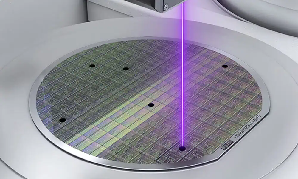
Polished, oxidized, deposited or patterned silicon can respond through surface films rather than bulk silicon. Control contamination, edge exclusion, wafer bow, backside support and the allowed heat-affected zone.
View the silicon wafer guide →Ceramic substrates
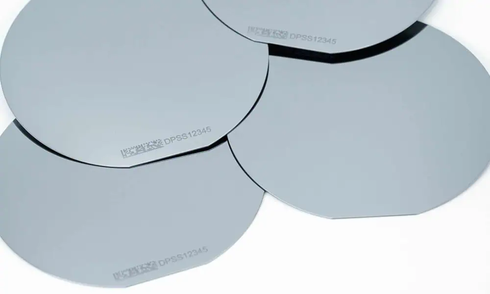
Alumina, aluminum nitride and other technical ceramics differ in porosity, glaze, metallization, thermal conductivity and surface roughness. Check chipping, edge breakout, conductor adhesion and cleaning after marking.
View the ceramic substrate guide →Solder mask and coatings
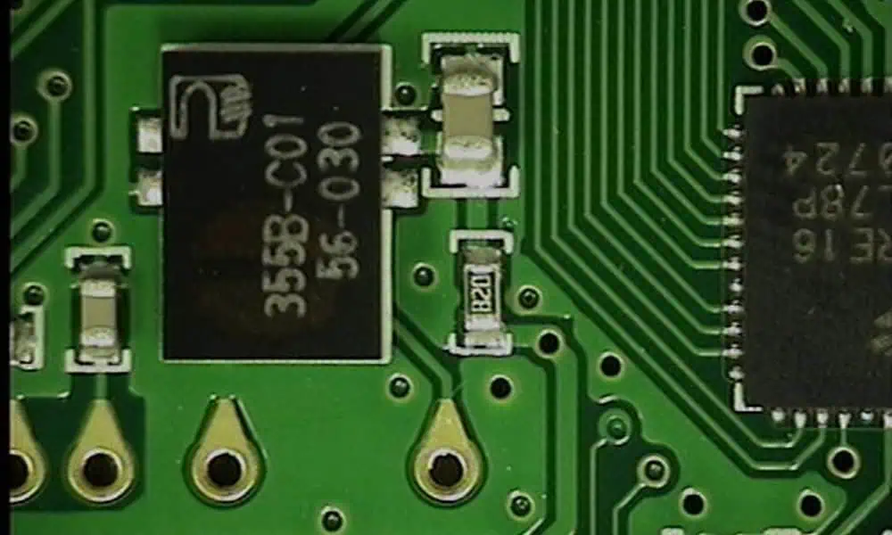
Mask color, resin chemistry, ink, legend print, copper exposure, cure state and board finish determine whether the laser creates contrast, removes a layer or damages the board. Identify the complete PCB stack.
View the solder-mask guide →Sapphire and display glass
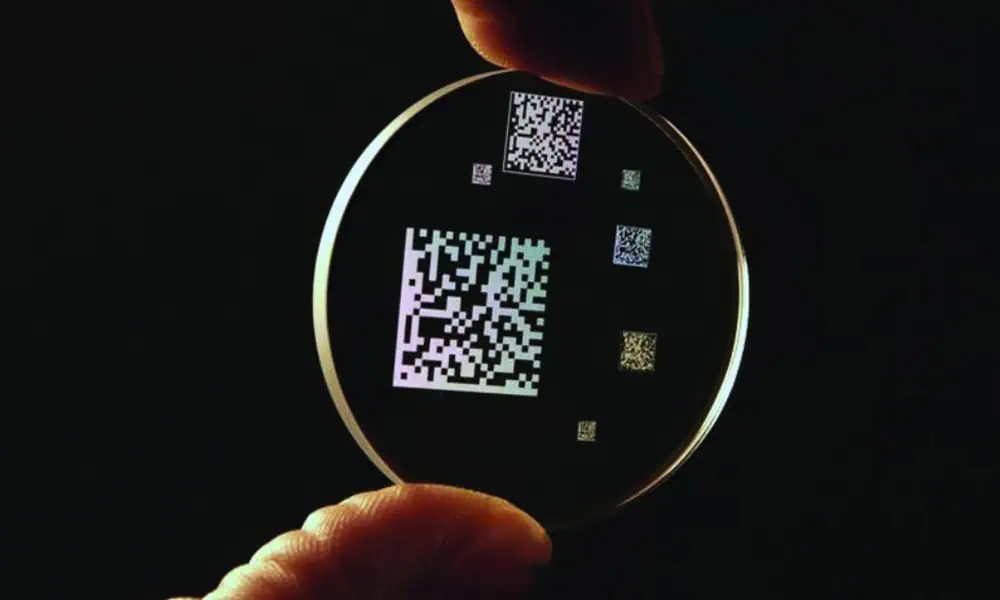
Transparent, polished or coated surfaces are sensitive to focus, stress, haze and microfracture. Cover glass, sapphire windows and display stacks need final geometry, optical condition and cosmetic limits in the test.
View the sapphire & display-glass guide →Behavior map
Map the layer, energy path and visible result
Before comparing machine wattage, record the layer that absorbs the beam and the layer that must remain unchanged. This prevents a good-looking coupon from masking delamination, conductor damage or hidden optical defects.
| Material variable | Typical process question | Failure signal | Acceptance evidence |
|---|---|---|---|
| Silicon surface film | Is the mark on oxide, nitride, metal or exposed silicon? | Film lift, debris, wafer edge damage or contamination | Microscopy, particle check, electrical/functional boundary and repeatability |
| Ceramic body and metallization | Will the mark stay within the ceramic or affect fired/conductive layers? | Chipping, microcracks, conductor lift, rough recast | Cross-light inspection, adhesion/cleaning check and dimensional limit |
| Solder mask / legend | Is the desired result contrast, selective removal or exposed copper? | Mask undercut, copper exposure outside artwork, residue or discoloration | Trace width, insulation boundary, contrast, cleanability and inspection grade |
| Sapphire / display glass | Can the surface be frosted or ablated without optical or structural damage? | Haze halo, star cracks, edge fracture or coating delamination | Cosmetic zone, transmittance/haze check, microscope review and thermal cycling if required |
| Coating, print or adhesive | Which layer creates the contrast and what fumes/residue are produced? | Uneven removal, odor, redeposition, unknown restricted substances | Layer specification/SDS, capture verification, residue and appearance limit |
Application context
Why Are Electronic Substrates Marked?
Laser marking is usually used when an electronic component needs permanent identification, traceability, inspection references or controlled surface modification without adding labels or inks. The exact reason depends on the substrate and where the mark sits in the finished component.
Silicon wafers & devices
Wafer and device surfaces may need lot, part or orientation identification, compact codes or process-reference marks. The mark must remain inside the allowed edge, contamination and thermal limits of the actual wafer or device stack.
Ceramic circuit substrates
Alumina, AlN and related substrates are used in electronic modules, power electronics, sensors and circuit carriers. Marking can support part identification, traceability and assembly control while avoiding cracks, conductor damage or residue.
PCB masks & coatings
Solder mask, legend and other board coatings may be marked for board identification, serialisation, traceability codes and inspection references. The process must distinguish harmless contrast from unwanted copper exposure or mask undercut.
Sapphire & display glass
Optical windows, covers and display-related parts may require discreet identification, alignment references or controlled cosmetic marks. Haze, microfracture, coating damage and edge stress can be more important than the visible mark alone.
Typical marking content
What Is Usually Marked?
The artwork itself changes the process requirement. A large logo, a small serial number and a dense machine-readable code do not demand the same spot size, scan strategy or inspection method.
Part & lot identification
Part numbers, serial numbers, lot or batch identifiers and other manufacturing references.
Machine-readable codes
1D or 2D codes such as Data Matrix or QR-style identification when the product and inspection method call for them.
Text & logos
Branding, component identification, polarity or orientation information and other readable text.
Fiducials & reference marks
Alignment, positioning or inspection references where a controlled mark is part of the manufacturing or quality process.
Target marking result
What Result Do You Actually Need?
“A visible mark” is not a complete specification. Decide whether the laser should change colour, remove a controlled layer, create texture or produce a code that remains readable without damaging electrical, optical or mechanical function.
High contrast, little removal
Useful when identification must be easy to see while keeping the substrate or coating largely intact. Validate colour consistency, heat effects and functional boundaries.
Selective layer removal
Used when a mask, coating, ink or film must be removed in a controlled area. Check depth, undercut, residue and whether the layer below is intentionally exposed or must remain protected.
Frosting or micro-texture
Relevant to selected glass, sapphire or ceramic surfaces where the visible effect comes from controlled surface modification. Inspect haze halo, roughness, cracking and edge sensitivity.
Readable fine features
Micro text and dense codes put more pressure on spot size, focus stability, scan strategy and inspection. Define the smallest feature and the acceptance method before choosing optics.
Part geometry
How Do Thickness, Size and Shape Change the Process?
Geometry changes focus, heat flow, stress, support and the motion needed to reach the full mark area. The same material can require a different machine configuration when the part changes from a small flat coupon to a thin wafer, large panel or curved optical cover.
| Part condition | What can change | What to evaluate |
|---|---|---|
| Thin wafers or brittle substrates | Backside support, local heating and edge stress become more critical. | Fixture flatness, bow, edge exclusion, thermal margin and crack/chip inspection. |
| Thick or heat-spreading parts | The energy needed for the target effect can change because heat leaves the mark zone differently. | Repeatable contrast/removal, local temperature effect and whether the process window is stable across the part. |
| Large panels or large mark areas | A single scan field may not cover the full required area at the needed feature size. | Lens/field choice, XY motion or indexing, stitching tolerance and fixture repeatability. |
| Curved, stepped or height-varying surfaces | Focus can move outside the useful depth of field. | Focal tolerance, part presentation, 3D focus or controlled motion where justified by the actual geometry. |
| Marks close to edges or fragile features | Crack, breakout, haze or coating-lift risk can increase. | Edge distance, local stress, support method, scan direction and acceptance under magnification. |
First screening route
Which Laser Route Should You Test First?
UV is often a sensible first screen for fine, low-heat features on selected coatings, silicon films and glass-like surfaces. CO₂, green or fiber/MOPA may be evaluated when absorption and the desired effect support them. The actual wavelength, pulse behavior, optics, field and enclosure must be confirmed on production samples.
- UV: fine text, micro codes and selected low-heat coating or glass trials.
- CO₂: conditional review for suitable coatings, ceramics or larger visible effects where heat can be controlled.
- Green: project-specific screening on transparent or reflective stacks when sample response supports it.
- Fiber/MOPA: selected metalized, conductive or additive-assisted layers; not a default for bare clear glass or every ceramic.
| Route | May be screened for | Boundary |
|---|---|---|
| UV | Fine marks, coating contrast, selected glass/silicon films | Focus, contamination, scan speed and coating chemistry still control the window. |
| CO₂ | Selected ceramics or polymeric masks/coatings, larger marks | Thermal spread, residue and conductor/optical damage must be checked. |
| Green | Conditional transparent/reflective stack trials | Use only with real sample evidence; no universal glass claim. |
| Fiber/MOPA | Conductive, metalized or additive-assisted layers | Bare silicon, ceramic and clear glass response is surface-dependent. |
Risks & failure modes
Check Mark Quality, Component Function and Safety Together
Electronic substrates can fail in ways that are not obvious from the front of the mark. Typical risks include microcracks, chipping, coating lift, copper or conductor damage, optical haze, residue and contamination. Plume, particles and reflected laser energy also have to be controlled. Evaluate the complete machine safety strategy—including enclosure, interlocks, extraction and wavelength-appropriate controls—for the actual equipment and material stack.
- Identify mask, ink, adhesive, metallization and unknown surface treatments; request supplier information or SDS where available.
- Verify enclosure airflow and plume capture at the actual mark, not only at the extraction inlet.
- Inspect particles and redeposition on optics, fixtures and product surfaces after repeated cycles.
- Define interlocks, emergency stop, maintenance access and wavelength-appropriate protective measures with the equipment safety owner.
- Hold production approval if cracking, delamination, insulation loss, optical haze or contamination is outside the agreed limit.
Sample validation
Send the complete substrate and define what “good” means
A meaningful test uses production-grade material, finished surface condition and measurable acceptance. A bare coupon is not enough when the product has a mask, conductor, optical coating, adhesive, curvature or cleanliness requirement.
| Input | Provide | Why it matters |
|---|---|---|
| Material identity | Silicon grade/film stack; alumina, AlN or other ceramic; solder mask/legend; sapphire or display-glass type | Composition and layer response can change the source direction and heat limit. |
| Surface stack | Bare, oxide/nitride/metalized, coated, printed, plated, polished, textured or laminated | The outer layer may absorb the beam and determine contrast, residue and fumes. |
| Geometry | Wafer, panel, coupon, curved cover, thickness, edge exclusion, fixture and focal tolerance | Controls focus, stress, edge risk and motion/fixture direction. |
| Mark requirement | Logo, text, 1D/2D code, serial, alignment fiducial, smallest feature and target location | Defines spot size, scan strategy and inspection method. |
| Acceptance | Contrast or ablation limit, microscope/vision grade, electrical insulation, haze/transmittance, cleanability and durability | Prevents approving a visible mark that damages function or appearance. |
| Production context | Batch variation, expected cycle, stop-station or continuous process, reject rule and documentation boundary | Shows whether a standard marking station is sufficient or whether motion, vision, automation or integration needs to be evaluated. |
Final machine configuration
How Does the Sample Test Define the Machine You Need?
A successful sample test should do more than prove that a mark is possible. It should establish a repeatable process window and show which machine features are actually necessary for the production part.
| Test finding | Configuration decision | Practical implication |
|---|---|---|
| Wavelength and pulse behaviour produce the required effect with acceptable heat and damage margin | Laser source family and required operating range | Avoid choosing a source only by nominal wattage; retain the route that gives the stable quality window on the real stack. |
| Smallest feature, code density and mark area are confirmed | Lens, spot size, marking field and working distance | Balance field coverage against feature size and focal tolerance rather than selecting the largest field by default. |
| Part is thin, fragile, curved, large or position-sensitive | Fixture, support, rotary/XY/3D motion or focus strategy where required | Only add motion or special focusing when the real geometry cannot be handled reliably by a simpler setup. |
| Part position or mark location varies between cycles | Vision, alignment or part-presence functions when justified | Vision can help identify and locate parts, but it does not by itself solve large height variation or poor fixturing. |
| Material produces plume, particles or reflective hazards | Enclosure, extraction, filtration and safety controls | Size the safety and fume-control approach for the actual wavelength, material stack, access mode and maintenance process. |
| Required throughput and line interaction are defined | Manual station, indexed motion, conveyor/online marking or project-based integration | Use full cycle requirements—not scan speed alone—to decide whether a standard station or a higher-level integration review is needed. |
Frequently asked questions
Electronic substrates and coatings FAQs
Can silicon be laser marked?
Selected silicon surfaces can be marked, but the useful route depends on oxide, nitride, metal, resist, contamination, wafer geometry and the allowed heat-affected zone. Test the actual film stack.
Which laser is best for ceramic substrates?
There is no universal answer. UV, CO₂, green or fiber/MOPA may each be screened for different ceramic bodies, metallization and desired effects. Chipping, microcracks and conductor adhesion must be part of acceptance.
Can a laser mark solder mask without exposing copper?
Sometimes, but mask color, cure, resin, thickness and board finish control the window. Define the desired contrast or selective removal and inspect copper exposure, insulation boundary and residue.
Can sapphire or display glass be marked?
Selected surfaces can receive frosting, ablation or coating changes, but haze halo, microfracture, edge damage and optical performance must be checked on the final glass or sapphire geometry.
What should I send for a test?
Send production samples with the complete layer stack, dimensions, finish, mark artwork, smallest feature, acceptance limits, batch variation, cleaning method and relevant SDS or coating information.
How is the final machine configuration chosen after testing?
Use the proven sample window to define the source family, optics and field size, then add only the fixture, motion, vision, enclosure, extraction and integration functions required by the actual part geometry, positioning tolerance, safety needs and production cycle.
Sample qualification
Let the real substrate choose the laser route
Share the production part, layer stack, finish, geometry, mark artwork and measurable acceptance criteria. After sample validation, Zhuorui Laser can evaluate the source route, optics, marking field, fixture, enclosure/extraction and any required motion or vision functions before quoting the final configuration.
Request a QuoteOEM & Custom InquiryContact Us