Ceramic Substrate Laser Marking
Screen serial numbers, lot codes and 2D identification on the actual ceramic-substrate stack—not on the word “ceramic” alone. This page focuses on electronic and technical ceramic substrates used in electronic assemblies, rather than decorative ceramic products. The fired body, metallization, printed ink, protective coating or mask, code geometry and heat limits all change the process window.
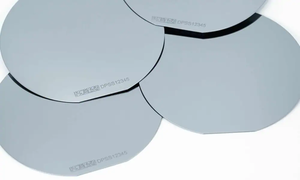
The hero graphic is illustrative. Final process selection requires the actual substrate stack and representative sample testing.
Can Ceramic Substrates Be Laser Marked?
Yes—many ceramic substrates can be laser marked for serial numbers, lot codes, text and 2D identification. The important question is not simply whether the product is “ceramic,” but which layer the laser must interact with: the fired ceramic body, a polished or coated surface, metallization or plating, or a printed ink, protective coating or mask layer.
The target layer is clearly identified, the required mark can be produced without unacceptable heat or material removal, and the code remains readable without damaging nearby conductors, edges, sealing areas or other functional features.
Confirm the exact ceramic grade and finish, all surface layers, code geometry, mark location, defect limits and functional checks on representative parts. A visually clear mark alone is not enough for production approval.
Identify the Ceramic Body and Every Surface Layer
Use the same layer vocabulary in the sample request, drawing review and acceptance record. “Ceramic substrate” without the stack is not enough to predict contrast or damage.
Ceramic body
Record alumina, aluminum nitride, LTCC, HTCC or another grade, plus purity, additives, color, density and firing history where known.
Surface finish
Separate as-fired, ground, lapped, polished, glazed and coated states. Gloss, roughness and focus tolerance can change the visible mark.
Conductor layer
Identify thick-film or thin-film metallization, plating and conductor clearance. The conductor may be the target—or a keep-out zone.
Ink, coating and residue
Document printed ink, protective coatings or masks—including solder-mask-type layers where applicable—plus adhesive, flux, oil and cleaning state. A surface layer can absorb differently from the ceramic beneath it.
| Family | Why it may differ | What to verify |
|---|---|---|
| Alumina (Al2O3) | Purity, additives, color and surface finish can change absorption, contrast and edge response. | Grade, fired condition, mark zone, contrast and microcrack/edge inspection. |
| Aluminum nitride (AlN) | Thermal conductivity and surface finish may change heat spreading and local response. | Grade, thickness, thermal/function limits and post-mark inspection. |
| LTCC / HTCC | Co-fired layers and internal conductors create stack and keep-out constraints. | Cross-section or layer drawing, conductor clearance and debris limit. |
| Metallized technical ceramic | The conductor, plating, ink or interface may be the actual marking target. | Layer identity, adhesion/electrical check, residue and cleaning method. |
Where Are Ceramic Substrates Used—and Why Are They Marked?
Ceramic substrates are used in electronic assemblies where insulation, thermal management, dimensional stability or circuit integration matter. The marking task is usually tied to traceability, assembly control or machine-readable identification rather than decoration.
Electronic and technical assemblies
- Power-electronics and thermal-management assemblies
- Thick-film and hybrid circuits
- Sensor and control modules
- LED and optoelectronic packages
- Metallized ceramic components and subassemblies
Identification that survives production
- Lot and batch traceability
- Serial identification and record linkage
- Part, revision or process identification
- Orientation and assembly reference
- 2D codes for inspection and downstream tracking
What Is Usually Marked on Ceramic Substrates?
The required content changes the process window. A short text string, a dense Data Matrix and a larger identification symbol do not have the same feature size, contrast or verification requirements.
Serial numbers
Unique part or substrate identification for traceability, inspection records and downstream assembly matching.
Lot and date codes
Batch, production-date or process codes used to connect physical parts with manufacturing and quality records.
2D identification
Data Matrix or other machine-readable codes where cell size, quiet zone, contrast and reader conditions must be defined before testing.
Part and assembly marks
Part numbers, short text, symbols, orientation marks or reference features used during inspection and assembly.
What Marking Result Do You Need?
Define the acceptance target before comparing lasers. “Readable” may mean visual contrast, repeatable machine decoding, controlled coating removal or a shallow surface change that does not compromise the substrate.
Code readability
Set the scanner or verifier, lighting, working distance and pass/fail rule. A code that decodes once is not the same as a repeatable production result.
Surface effect
Choose the intended effect: contrast change, coating removal, shallow texture or controlled ablation. Do not assume every ceramic body can produce the same dark or light appearance.
Functional integrity
Keep conductors, pads, vias, seal areas and critical edges within defined limits for heat, particles, material removal and mark depth.
Durability
Test realistic handling, cleaning, solvents, thermal cycling or downstream assembly when the code must remain readable after those conditions.
How Do Thickness, Size and Geometry Change the Marking Process?
Part geometry does more than change fixture dimensions. It affects heat spreading, edge risk, focus consistency, field coverage and how reliably the same code can be placed from part to part.
Thin substrates and edge zones
Thin parts and marks close to an edge deserve tighter control of local heat input, clamping and inspection because chipping, cracking or distortion may become more consequential.
Large panels
A larger marking area changes field-size selection, optical distortion, flatness tolerance and positioning strategy. The required code quality must hold across the usable field, not only at the center.
Warped or uneven surfaces
Height variation changes focus. Fixture datum, focus tolerance, autofocus or other compensation may need to be evaluated when the mark zone cannot stay within a stable focal plane.
Small or mixed-orientation parts
Repeatable location can depend more on fixture datum, part orientation and vision positioning than on the laser source itself, especially when codes must align with pads, edges or assembly features.
Which Laser Route Should You Test First?
Start from the target layer and acceptance risk, then compare only the laser families that have a plausible interaction with that layer. The first test route is a screening direction—not a universal machine prescription.
| Actual target | First route to screen | Why start there | What must decide the result |
|---|---|---|---|
| Bare ceramic body with fine text or 2D code | UV is a sensible early comparison on many projects; add another route only if the sample response justifies it. | Fine-feature control and a tighter thermal window are often the first concerns. | Contrast, code readability, edge quality, debris and microcrack inspection on the actual grade and finish. |
| Metallized or plated surface | Compare fiber/MOPA and UV when both are plausible for the specific metal/ceramic stack. | The key question is layer selectivity: producing the code without unacceptable conductor, adhesion or interface damage. | Electrical or adhesion checks where relevant, residue, heat effect and code quality. |
| Printed ink, protective coating, mask or other surface layer | Screen UV or CO2 when the layer chemistry and thermal limit make them plausible; add fiber/MOPA only when actual surface response supports it. | The interaction may be surface-layer contrast or controlled removal rather than modification of the ceramic body. | Clean removal or contrast, residue, edge definition, adhesion and damage to the underlying layer. |
| LTCC / HTCC or multilayer structure near conductors | Begin with the route that best matches the required feature size and functional heat limit; UV is often worth an early comparison for fine coding. | Internal or nearby conductors make heat, depth and keep-out control more important than appearance alone. | Code readability plus functional inspection, debris and crack/delamination checks. |
| Unknown or mixed surface stack | Do not choose the laser first—identify the exposed target layer before testing. | A route selected from the word “ceramic” can be aimed at the wrong material interface. | Stack identification, target effect, keep-out zones and acceptance criteria. |
Green or other wavelengths can enter a project-specific comparison when absorption, feature size or thermal behavior gives a clear reason to test them. They should not be presented as the default simply because the substrate is ceramic.
Common Risks in Ceramic Substrate Laser Marking
A visually clear code is not enough if the process creates cracks, debris, delamination or functional change. Approve the mark and the substrate condition together.
Unreadable or unstable codes
Low contrast, damaged cells, inconsistent focus or changing surface conditions can make a code readable on one part and unreliable across a batch.
Chips, cracks and debris
Inspect edge roughness, chips, microcracks, particles and residue at useful magnification, especially near edges or on thin parts.
Layer or conductor damage
Metallization, plating, inks and interfaces can discolor, delaminate or change function if the process is not selective enough.
Functional change
Check insulation, conductor resistance, thermal path, sealing and assembly interfaces where the mark is close enough to affect them.
How Should a Real Ceramic-Substrate Sample Be Validated?
Use representative final parts—not a generic ceramic or PCB photo—to qualify the marking route. The test should reproduce the actual layer stack, code geometry, mark position and acceptance method closely enough to expose the real risks.
- Stack: body grade, thickness, finish, conductor/metallization, ink/mask and cleaning state.
- Mark: artwork or code, smallest cell, location, quiet zone and target effect.
- Geometry: drawing, flatness, edges, datum, fixture and allowed focus variation.
- Acceptance: reader/verifier, contrast, defect limits, durability and functional checks.
- Production: quantity, cycle target, loading, orientation, data source and inspection flow.
- Safety: SDS or restricted substances, fume/particle controls and operator constraints.
- The actual substrate family, surface condition and target layer used for the trial
- The mark content and representative images of the tested result
- Reader/verifier observations plus visible defect and functional-check status where relevant
- The preferred laser direction, remaining risks and configuration inputs needed for the quotation stage
Turn the Approved Sample into a Machine Configuration
After the representative substrate and code pass inspection, convert the test result into the optical, fixture, positioning, handling, verification and safety configuration needed for production. The same laser source can require a very different system around it for different ceramic parts.
| Input | Why it matters | Configuration decision |
|---|---|---|
| Approved laser route and target effect | Sets the source family and the process direction that has already passed sample screening. | Laser source / pulse behavior review |
| Code size and marking field | Changes optics, focus tolerance, distortion and cycle calculation. | Lens, field size and optical setup |
| Flatness, thickness and orientation | Determines datum strategy and whether focus variation must be compensated. | Fixture, focus and vision review |
| Loading and cycle target | Determines how the part is presented and whether indexing or automation is justified. | Manual, indexed or automated handling |
| Data and inspection | Defines code input, reader/verifier requirements and reject handling. | Software, reader and integration review |
| Fumes, particles and radiation | Sets enclosure, interlock, extraction and operator-control requirements. | Safety and extraction configuration |
Fiber/MOPA systems may use invisible near-infrared radiation (often around 1064 nm, source-dependent), while UV is also invisible to the eye. Metallized pads and plating can create specular reflections; use suitable enclosure, interlocks, beam control and fixture orientation before a trial. Open or accessible setups may require Class 4 controls, wavelength-matched eyewear, signage and access control. Review SDS and use local extraction/filtration for coatings, inks, adhesives or residues; automated cells need safe access and fault-stop logic.
Ceramic Substrate Laser Marking FAQs
Can ceramic substrates be laser marked?
Yes, many alumina, aluminum-nitride, LTCC, HTCC and metallized ceramic substrates can be evaluated for serial, text or 2D identification. Compatibility still depends on the exact body, exposed layer, code geometry and functional limits, so production approval requires representative samples.
Is UV always the best laser for ceramic substrates?
No. UV is often worth an early comparison for fine coding on bare or heat-sensitive stacks, while fiber/MOPA can be relevant to metallized or additive-responsive surfaces. CO2 or green may enter selected projects when the actual surface layer and absorption behavior justify them.
Can I mark the conductor on a ceramic substrate?
Sometimes the conductor or plating is the intended target, but selectivity, adhesion, resistance and debris must be checked. Treat conductors, pads and vias as functional zones until the test proves otherwise.
Does ceramic thickness or edge position affect the test?
Yes. Thin parts, marks close to an edge, warped substrates and large panels can change clamping, focus consistency, heat response and crack/chip risk. Include the final geometry and mark location in the sample trial.
How small can a Data Matrix be?
There is no universal size. Cell geometry, optics, contrast, surface response, placement tolerance, lighting and reader/verifier method all matter. Validate the complete code and inspection setup on the final part.
What should I send for testing?
Send representative final parts, stack information, drawing, code/artwork, target effect, reader/verifier rule, durability or function checks, cycle target, fixture constraints and relevant safety information.