
Applications · Electronics & Electrical
PCB and PCBA Laser Marking
Board-level traceability codes, solder-mask identification and production marking for electronics manufacturing. This page helps you define why the board is marked, what result is required, which variables and handling conditions affect the result, which laser direction to test first, how to accept the sample and how the test outcome determines the final machine configuration.
- Board-level QR / Data Matrix / serial-number traceability
- Position discipline across solder mask, FPC, metal-core and assembled PCBA
- UV cold-processing direction evaluated first, confirmed by sample testing
Quick Answer: PCB & PCBA Laser Marking at a Glance
Yes — laser marking is an established method for putting permanent identification on printed circuit boards. In electronics manufacturing, boards are commonly marked with QR codes, Data Matrix symbols, serial numbers, date and lot codes, and panel-level identifiers that survive reflow, washing and handling. The practical question is not whether it can be done, but what your specific board needs, where the mark can go, and which laser direction should be evaluated first.
This page covers the board-level application behind a PCB laser marking machine decision: why boards are marked, what gets marked on bare PCB, flex, metal-core, ceramic and assembled PCBA, which surface and geometry variables control the result, where the mark can go, which laser direction should be tested first, how the station fits into production, how samples should be accepted and how those results determine the final machine configuration. Detailed coating and substrate response remains available in the electronic-substrate material guidance.
Scope note: this page covers the board itself. Marking individual electronic components (IC bodies, capacitors, relays) is covered by the electronic component marking page, and connector / terminal marking by the connector and terminal marking page.
Why Are PCBs and PCBAs Laser Marked?
The mark is usually part of the manufacturing and traceability system, not decoration. Its job is to keep the board identity connected to the right production, test and service records.
- Unit traceability — give each PCB or assembled PCBA a unique identity that can be linked to batch, work-order and process records.
- Panel traceability — preserve the relationship between an individual board and the panel or array it came from before depaneling.
- Process and test linkage — connect the physical board to inspection, test, rework or disposition data in the production system.
- Revision and change control — distinguish part numbers, board revisions, ECO states or customer-specific versions during manufacturing and service.
- Mix-up prevention — reduce the risk of the wrong board, revision or production lot moving to the next process or customer order.
- Rework, return and service identification — keep a permanent identifier available when a board is repaired, returned or investigated later.
The required code format and data structure are defined by your production, quality or customer requirements. The laser system has to reproduce that information at the required position and quality without creating unacceptable board damage.
What Is Typically Marked on a PCB or PCBA
Board-level marking gives each board, panel or finished assembly a unique identity that can be scanned and linked back to production data.
Board-level traceability codes
The core of PCB traceability is usually a QR code or a Data Matrix symbol. The code can carry a unique identifier and, where required, selected structured production data. In many manufacturing traceability systems, that identifier is used to retrieve the board’s batch, work-order, inspection and test history from the MES or database rather than storing the complete production history in the code itself. A serial or lot number in readable text is frequently placed beside the code so operators can identify the board without a scanner.
Panel and array identification
Boards are usually manufactured as a panel containing multiple units. Each unit typically receives its own code, and the panel or array often carries a separate panel-level identifier, so the manufacturing history can be traced both at the unit level and at the panel level. The mark position differs depending on whether the code is applied before or after depaneling.
Assembly, customer and UID identification
Beyond traceability, boards are marked with assembly-related identifiers, customer part numbers, logos, version or ECO identifiers, and, in some regulated or program-driven supply chains, unique identification data defined by the buyer or applicable program. The required terminology, data structure, code format, size and location therefore come from the customer or governing specification, not from the marking machine.
Code formats and data sources
| Mark content | Typical format | Typical purpose |
|---|---|---|
| Board serial / lot number | Readable text | Unit identification, rework and return handling |
| Traceability code | QR / Data Matrix / GS1 DataMatrix | Full history link: batch, date, work order, test data |
| Panel / array ID | QR / Data Matrix + text | Panel-level history before depaneling |
| Date / ECO / version | Text | Revision and change control |
| Customer part number / logo | Text / graphic | Product identity and brand compliance |
| Program-defined unique ID / traceability code | Data Matrix or customer-specified format | Program / regulatory traceability |
In a typical traceability flow, the MES or serial-number database provides the unique identifier or encoded data to the marking software, the code is applied to the board, and a camera can verify that the marked code is readable and matches the expected data before the board moves on. Where required, the verification result or pass/fail status can also be returned to the production database. How this data flow is built — and whether your line needs it — is a project question covered by the traceability integration solution rather than by this application page.
What Determines Laser Marking Results on PCBs and PCBAs?
“PCB” is not enough information to select a process. The result changes with the exact surface, what lies below it, the code requirement, board geometry and the production steps the mark must survive.
Target surface, colour and formulation
Most bare-board marks are made on solder mask, but different mask colours, ink formulations, coating thicknesses, suppliers and batches can respond differently to the same laser settings. A recipe that works on one green mask should not be assumed to transfer unchanged to another colour or supplier. Exposed copper, aluminium, plated metal, ceramic and polyimide are different laser tasks and may point to a different wavelength or parameter window.
What lies below the marking surface
A solder-mask mark is made on a thin coating over the PCB stack-up. The underlying copper pattern, laminate, local layer structure and available mask thickness affect how much process margin you have before unwanted removal or thermal damage becomes a risk. Functional traces, pads and vias should be treated as keep-out features unless the design intentionally provides a tested marking area.
Code size, contrast and inspection requirement
A large readable serial number and a small machine-readable Data Matrix do not impose the same process window. Module size, required code dimensions, background colour, scanner or verifier, target grade if specified, and allowable visual change all influence the optical field, spot size and parameter development.
Board type and thermal sensitivity
Rigid FR-4 boards, FPC, metal-core boards, ceramic substrates and assembled PCBA do not present the same risk. Flex circuits are more sensitive to heat and movement; assembled boards add component proximity and height variation; metal-core and ceramic boards change both heat flow and surface response. These differences affect both the laser route and the way the part is supported.
Flatness, warpage and focus stability
Panel bow, flexing, fixture tolerance and assembled-component height can move the marking surface away from the intended focal plane. Vision can correct X-Y position when the board shifts, but it does not by itself correct height or focus variation. Where Z variation is significant, fixture design, controlled support, autofocus or another height-control strategy may need to be evaluated.
Downstream process and batch variation
Reflow, cleaning, conformal coating, handling and later assembly steps can change how the mark is read or whether it remains accessible. If several solder-mask colours, suppliers or board revisions are used, the sample plan should include the variants that matter rather than validating only one convenient board.
How Do Board Geometry, Panelization and Handling Affect Marking?
A good laser recipe still fails in production if the board cannot be presented at a repeatable position and focal height. Marking area, board support and handling method therefore belong in the machine decision.
The practical rule is to use a dedicated marking area with enough clearance from functional features. Functional traces, pads, vias, solder joints and sensitive components should be treated as keep-out features unless the PCB design intentionally provides a separate exposed-metal marking target that has been validated for laser processing.
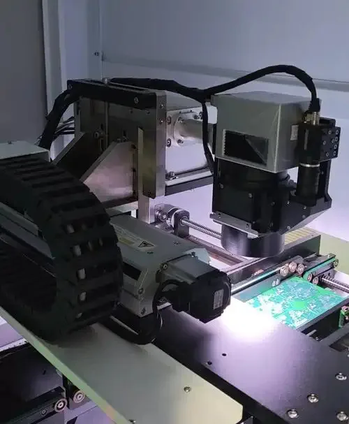
Engineering takeaway: board positioning and available marking area must be reviewed before marking; final contrast and process settings still depend on the actual solder mask, board finish and marking requirement.
Safe zones and keep-out zones
- Dedicated solder-mask blank area — a common target for bare-board codes when sufficient clearance from functional copper and other features is available.
- Panel blank, process rail or edge area — useful for panel-level identifiers and for codes applied before depaneling.
- Component-free area on assembled PCBA — mark only where the design provides clearance from nearby devices and solder joints.
- Functional traces, pads, vias and ground features — normally keep out of the marking area unless the design explicitly defines and validates another target.
- Repeatedly flexed zones — avoid placing the mark where bending can later crack or delaminate the marked surface.
- Areas covered later — for conformal coating, define whether the code must remain readable after coating; for potting, determine whether verification must occur before the board becomes inaccessible.
Single board, panel or array
A stable single board may need only a mechanical fixture. A panel or array adds board-to-board pitch, panel distortion, fiducial location, depaneling tolerance and repeated marking positions. If those positions vary beyond fixture repeatability, camera-based alignment becomes useful for X-Y correction.
Rigid PCB, FPC and assembled PCBA
Rigid boards are usually easier to support flat. FPC may need vacuum support or a dedicated nest so the surface does not move or bow during marking. Assembled PCBA adds component height and possible Z variation, so the laser head, working distance and fixture must maintain focus without risking collision with tall components.
Loading, changeover and side access
Manual loading, trays, panel conveyors and automated transfer place different demands on the fixture and available working envelope. If several board sizes or product variants share one station, changeover time, recipe selection and fixture repeatability should be part of the evaluation rather than treated as an afterthought.
For alignment methods, see the vision positioning solution.
What Marking Result Should You Target on a PCB or PCBA?
A “visible mark” is not a useful acceptance target. Define what the code must do, what surface change is acceptable and what damage is prohibited before comparing laser settings or machines.
- Reliable readability — text must remain legible and machine-readable codes must decode with the intended scanner or verifier.
- Defined code quality — if your quality system specifies a grading method or minimum grade, use that requirement as part of the sample acceptance criteria rather than assuming visual contrast is enough.
- Controlled surface change — the mark should create the required contrast without unacceptable charring, halo, excessive mask removal or other cosmetic change.
- No unacceptable functional damage — the tested process must not expose or damage functional copper, pads, vias, laminate, solder joints or nearby components.
- Position accuracy — the complete code must remain inside the designated marking area with the required clearance from keep-out features.
- Process survival — readability must remain acceptable after the downstream steps that matter to your process, such as reflow, cleaning, handling or conformal coating.
- Repeatability across real variation — the result should remain acceptable across the board colours, suppliers, batches or product variants included in the project.
- Production-capable cycle — mark quality is not enough if loading, positioning, marking and verification cannot meet the required station cycle.
Define the target before testing: code format and size, required reading or grading method, allowed visual change, prohibited damage, position tolerance, downstream survival checks and target cycle time. Those criteria turn a sample from a visual demonstration into an engineering decision.
UV vs. Fiber Laser for PCB and PCBA Marking
For the surfaces found on boards, two laser directions cover most cases. The choice is conditional — and the final result on your specific board must be confirmed on a real sample.
UV (~355 nm) — the usual first evaluation for solder mask, FPC and ceramics
UV lasers are commonly the first direction evaluated for PCB marking, for one reason: the short wavelength is absorbed strongly by many solder-mask inks and polymer surfaces, producing a clean, high-contrast mark with a smaller heat-affected zone than infrared sources. This matters for fine codes on dense boards, for heat-sensitive flex circuits, and for ceramic substrates that take a dark, legible mark. “Cold marking” describes the effect, not a complete absence of thermal influence — the useful parameter window still has to be found for each mask colour and thickness, and confirmed on samples.
Fiber (~1064 nm) — for exposed metal surfaces, with a caution on solder mask
Fiber lasers are the standard tool for metal marking, and they are a reasonable direction when the target is an exposed copper or aluminium surface, a metal stiffener, a shielding cover or a metal frame on the assembly. On solder-mask surfaces, however, the infrared wavelength is absorbed less efficiently and the heat can accumulate — raising the risk of damaging the mask, the laminate or nearby features. If a fiber source is considered for a mask surface, it should be evaluated on the actual board material rather than assumed.
MOPA, CO₂ and green — conditional, by surface
MOPA fiber lasers bring a wider pulse-width and frequency window, which can help on some coated or metal surfaces where contrast or heat control matters. CO₂ lasers are not a common first choice for fine, high-density PCB codes but can appear for larger organic-surface tasks. Green lasers appear in specific material cases — for example, some coated or plated surfaces where wavelength-specific absorption is under evaluation. Each of these is a conditional evaluation driven by the actual board surface and target mark, not by default.
Parameter direction — why not just pick a power
Average power alone does not determine a good PCB mark. The usable process window has to balance contrast, code edge quality, surface removal and thermal load on the actual board. Pulse energy, repetition rate, scan speed, hatch, number of passes, focus and field size can all change that balance, and the useful combination depends on the mask or substrate being marked. This is why a parameter recipe for your board is developed during sample testing rather than copied from a catalogue or reduced to one power value.
What Are the Common PCB and PCBA Laser Marking Failure Modes?
A failed sample does not always mean the laser technology is wrong. The failure pattern helps identify whether the next change should be the wavelength, process window, optics, positioning, fixture, verification or production architecture.
| Failure | What to review next |
|---|---|
| Weak or inconsistent contrast | Actual mask formulation or colour, wavelength, focus, parameter window, surface contamination and supplier / batch variation. |
| Code is visible but does not decode reliably | Module size, edge definition, contrast uniformity, quiet zone, optics / field size, verifier setup and code-generation quality. |
| Excessive mask removal, halo or charring | Thermal load, pulse / scan strategy, focus, wavelength choice and whether the requested contrast is realistic on that surface. |
| Copper or laminate becomes exposed or damaged | Marking-zone design, underlying stack-up, process energy and keep-out clearance. Do not solve this by simply accepting a darker mark. |
| Position shifts between boards or panels | Fixture repeatability, fiducial strategy, panel distortion, camera alignment and part-present / orientation checks. |
| FPC moves, bows or marks inconsistently | Support method, vacuum or nest design, surface flatness and focus stability. |
| Mark passes initially but degrades after production | Reflow, cleaning, coating, handling sequence and whether acceptance was tested at the correct process stage. |
| MES value, marked code and verification record do not match | Data handshake, serialization logic, camera read-back, pass/fail logic and record association. |
| Mark quality passes but the station misses takt time | Full cycle time: loading, locating, marking, verification, unloading, conveyor transfer and changeover — not scan speed alone. |
How Does PCB Laser Marking Fit Into Production?
The station architecture is decided by where identification belongs in your process, how boards are handled, how data is assigned and verified, and what cycle time the line can accept.
Offline benchtop marking
An offline machine suits low-to-mid volumes, frequent changeovers and mixed board types. Boards are loaded by an operator, positioned by a fixture or a small vision system, marked, verified and unloaded. It is the simplest path to start PCB marking, and it can still carry MES connectivity through the marking software even when the boards move by hand.
Inline at the defined production stage
When boards move in a continuous production flow, an inline station can be placed at the production stage where the identifier must be created and verified. Depending on whether the target is a bare PCB or an assembled PCBA, that point may be before assembly, after a defined process step or later in the line. The station can receive the code value from the MES or database, position the board, mark it, verify the result and return the pass/fail record before release to the next operation.
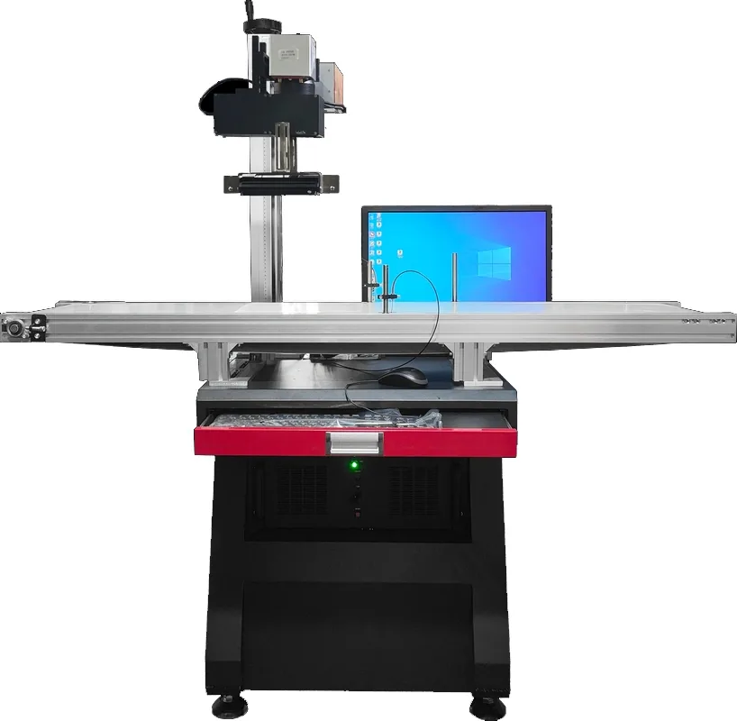
Engineering takeaway: conveyor handling is only one part of an inline marking station; board positioning, code generation, verification and line-cycle requirements still need to be defined for the actual PCB process.
Throughput and changeover considerations
The real cycle includes loading, positioning, marking, verification and unloading — not just the laser scan time. Inline systems add conveyor timing, panel-to-panel changeover and line-speed matching to that total. A project evaluation has to confirm that the marking station can keep up with the line without becoming the bottleneck, and that the MES or database interface matches your existing control environment. These integration questions are evaluated as a project; the flying / online marking solution, automatic loading solution and traceability integration solution pages explain the system methods.
How Should PCB and PCBA Marking Samples Be Accepted?
Agree the pass/fail criteria before the sample test. Otherwise a visually attractive mark can be approved even though it does not satisfy the real production requirement.
Readability and code-quality acceptance
Confirm the actual text, QR or Data Matrix size with the scanner or verifier that matters to your process. If your quality system requires a specific grading method or minimum grade, define that requirement in advance and record the result on the marked sample.
Surface and damage acceptance
Define what visual change is acceptable and what is prohibited. Inspect for excessive solder-mask removal, halo, charring, exposed copper, laminate damage and any effect on nearby pads, vias, solder joints or components. The acceptance rule should be based on the functional and cosmetic requirement of the board, not only on whether the code can be seen.
Position and repeatability acceptance
Check that the complete mark stays inside the defined marking area and keeps the required clearance from functional features. Repeat the test across enough boards or panel positions to reveal fixture, alignment or panel-distortion problems rather than approving a single best sample.
Downstream-process acceptance
Verify the mark after the production steps that can change readability or access. That may include reflow, cleaning, handling and conformal coating. If the board will later be potted or otherwise made inaccessible, decide whether the identifier must be verified before that step or whether another external identifier is required.
Variant and cycle-time acceptance
Include the solder-mask colours, suppliers, board variants or revisions that materially change the process. Then measure the complete station cycle — loading, positioning, marking, verification and unloading or transfer — so a passing optical result is not mistaken for a production-capable process.
A useful sample-test record should contain: board / surface identity, mark content and size, target acceptance criteria, laser route tested, inspection method, downstream checks, observed failure modes and full-cycle requirement. Exact commercial parameter recipes can remain project-specific; the acceptance result still needs to be clear enough to choose the final equipment architecture.
How Do Sample-Test Results Determine the Final Machine Configuration?
The final machine should be the consequence of the accepted sample and production conditions. Laser source, optics, positioning, fixture, handling, verification and data functions are selected from what the test proves — not from the word “PCB” alone.
| Sample or production finding | Configuration implication |
|---|---|
| UV produces the required contrast on solder mask or FPC with acceptable surface change | Keep UV as the source route and define the source / optics / parameter window around the accepted sample rather than switching technology for nominal power alone. |
| An exposed copper, aluminium or other metal target performs better with fiber | Use the tested fiber route for that intentional metal marking area and keep mask-surface assumptions separate. |
| The required code is very small or edge definition drops when the marking field is enlarged | Revisit lens / field size, spot size and optical layout. The largest field is not automatically the best field for a fine code. |
| Board or panel X-Y position varies beyond fixture repeatability | Add fiducial or vision alignment and define the recognition / correction logic. |
| FPC cannot remain flat or panel warpage moves the surface out of focus | Improve the fixture / vacuum support and evaluate Z-height or focus-control requirements; vision alone does not correct height variation. |
| Assembled PCBA has tall components or variable marking height | Check working distance, collision clearance, Z adjustment / autofocus strategy and whether the selected head arrangement can access the mark safely. |
| Mark quality passes but full cycle time fails | Review marking field, recipe, loading, conveyor transfer, positioning and verification architecture before simply increasing laser power. |
| Code values must come from MES and every board needs read-back confirmation | Add the required data interface, serialization control, camera verification, pass/fail handling and result logging. |
| Several board sizes or frequent product changes share one machine | Plan adjustable or interchangeable fixtures, recipe management, vision as needed and conveyor / working-area range for the product family. |
Information to send with the sample or RFQ
With those inputs, the project can move from “we need a PCB laser marker” to a specific source route, optical field, fixture / vision strategy, handling method, verification method and offline or inline machine configuration.
- Board type, dimensions and whether it is bare, flex, metal-core, ceramic or assembled
- Exact marking surface, solder-mask colour / finish and relevant supplier or batch variants
- Mark content, code format, target code size and any grading / readability requirement
- Available marking area, underlying / nearby features and keep-out rules
- Panelization, flatness / warpage concerns and loading method
- Required throughput or station cycle and changeover pattern
- Production point for marking, downstream processes and verification timing
- MES / database / camera / pass-fail interface requirements
- Samples that represent the actual variants to be qualified
FAQ
Can a laser mark on green solder mask without damaging the board?
Yes — green solder mask is the most common surface for PCB laser marking, and a clean, readable mark is typically achievable with the right parameters. The result depends on the mask colour, thickness and board batch, so it should be confirmed on a real board sample.
Why is UV laser often recommended for PCB marking?
UV light is strongly absorbed by many solder-mask inks and polymer surfaces, which gives a clean, high-contrast mark with a smaller heat-affected zone than infrared sources. That is why it is commonly the first direction evaluated for mask, flex and ceramic surfaces — the final recipe still needs sample confirmation.
Can a fiber laser mark on copper or aluminium-core PCBs?
Fiber lasers mark exposed metal surfaces well, so they can be a reasonable direction for copper, aluminium-core or metal-stiffener targets. On solder-mask surfaces, the infrared wavelength is absorbed less efficiently and heat can accumulate, so a fiber source on a mask should be evaluated on the actual board rather than assumed.
What is the smallest QR or Data Matrix code that can be marked on a PCB?
The minimum readable code size depends on the spot size, the marking optics, the surface contrast and the scanning hardware used — it is configuration-dependent. For your required code size and grade, the practical answer is confirmed by marking and reading samples on your actual board.
Does laser marking survive reflow and washing?
Laser marks are permanent surface modifications rather than printed layers, so they generally survive soldering and cleaning processes — but the exact survival depends on the surface, the mark depth or contrast, and the process temperatures. Readability should be verified after your real production steps.
Can laser marking be integrated with MES for inline traceability?
Yes — an inline station can receive code values from the MES or a database, mark each board, verify the code and return the result to the system. This is a project-level integration that depends on your line layout, control environment and data requirements.
Ready to Evaluate PCB & PCBA Laser Marking for Your Line?
Send your board type, solder-mask colour, mark content and target code size, and we will review the application, confirm the laser direction and prepare a sample marking test.