
Material response · coating boundary
Solder Mask Laser Marking: Control Color Change and Ablation Boundaries
Yes—laser marking can be evaluated on cured solder mask, but a readable mark is not automatically an acceptable one. The usable result depends on the actual mask formulation and color, cure, thickness, surface condition, and the copper or laminate beneath it. The first decision is whether you need visible contrast while keeping the mask functionally intact, or deliberate mask removal to a defined stopping layer.
Define the stopping boundary
Representative engineering diagram — not a tested board cross-section.
Process-window variables
The finished surface stack—not the board name—controls the response
Two boards both described as “green PCB” can react differently. Record the actual solder-mask product or family, color, cure, thickness, surface condition and underlying layer before comparing a laser source or parameter window.
Mask chemistry and color
Resin, pigment, filler and supplier formulation change absorption, contrast, plume and residue. Color is a screening clue, not a process specification.
Cure and thickness
Under-cure, over-cure, thickness variation and rework can change color response, ablation threshold, edge quality and the margin before layer breakthrough.
Underlying layer
Copper, surface finish, laminate, vias and nearby conductors change heat spreading and the consequence of breakthrough. Define what may and may not be exposed.
Legend ink is a separate layer
Legend / silkscreen ink, conformal material, contamination, cleaning residues, texture and gloss can change the top-surface interaction. Do not treat white or black legend printed over solder mask as if it were the solder mask itself; record and test the layers separately when the mark crosses both.
| Variable | What may change | Failure signal | Test control |
|---|---|---|---|
| Mask formulation or color | Absorption, contrast, plume and residue | Low contrast, scorching, uneven tone or redeposition | Separate samples by supplier, product and color; do not pool results. |
| Cure and thickness | Threshold and margin before breakthrough | Pinholes, unexpected exposure, ragged edge or incomplete removal | Use production-cured boards and include known thickness variation. |
| Copper / surface finish / laminate below | Heat flow and stopping-layer response | Copper attack, discoloration, lifted edge or laminate damage | Map the artwork to the real stack and inspect the layer below. |
| Legend / overprint / contamination | Top-layer absorption, local contrast and removal sequence | Patchy result, false edge, legend-first removal or cleaning-dependent appearance | Test bare solder-mask areas and legend-covered areas separately when both occur in the artwork. |
Application context
Where is solder-mask laser marking used—and why?
Laser marking is considered when a PCB or PCBA needs permanent identification directly on a production-finished board surface. The material question is whether the required contrast or removal can be created without compromising the solder-mask function or the layer below.
PCB and panel identification
Board makers and electronics manufacturers may need a permanent identifier on individual boards or on panels before singulation. The mark location must stay compatible with pads, vias, copper features and later assembly operations.
Product and process traceability
Serialized or lot-specific marks can connect a board to production, inspection or service records. The material page determines whether the surface can carry the mark; data binding, readers and MES logic are separate production-system decisions.
Readable information without an added label
Direct marking can be evaluated where labels, extra printing steps or removable identifiers are undesirable. The requirement should still be defined by readability, durability and board-function limits—not by appearance alone.

Marking content
What is usually marked on solder mask?
The artwork changes the optical and positioning requirements. Large human-readable text is a different process problem from a dense machine-readable code with small modules and tight quiet-zone requirements.
2D codes and serialized identification
Data Matrix, QR codes and other project-specified machine-readable identifiers may be used for traceability. Define the code size, module or cell size, quiet zone, required reader and verification method before selecting the final field and optics.
Text, part information and symbols
Part numbers, revision identifiers, serial numbers, inspection identifiers, symbols and other human-readable information can be evaluated where the board layout allows it. Small strokes, dense graphics and mixed legend/solder-mask areas need more careful focus and edge control.
Do not mix content with surface identity: a printed legend may already contain reference designators and symbols, but laser marking the solder mask is a separate process. If the laser artwork overlaps legend ink, test that stack as a distinct condition.
Answer first
Define the marking result before choosing the laser
For a laser-marking project, the usual first target is controlled visible contrast while keeping the solder mask functionally intact. Deliberate solder-mask ablation is a separate processing target with different stopping-layer and inspection requirements.
Controlled visible contrast
Create readable optical contrast without intentionally opening the solder mask. Approval should include contrast or code readability plus checks for halo, gloss shift, roughness, thinning, pinholes and unintended copper exposure.
Controlled solder-mask ablation
If the requirement is to remove mask and expose a defined area or stopping layer, treat it as an ablation task rather than ordinary identification marking. Edge position, undercut, residue, exposed area and the condition of copper or laminate become primary acceptance criteria.
Board condition and geometry
How do PCB construction, size and flatness change the result?
The same solder mask can behave differently when the focal height, support condition, underlying copper pattern or mark location changes. These factors also determine whether a simple marking station is enough or whether Z control, vision or custom fixturing should be evaluated.
Mask thickness
Thickness changes the margin between a useful surface response and unwanted breakthrough. Use production-cured boards and include normal thickness variation in the test matrix.
Board flatness and warpage
Height variation moves the surface away from the calibrated focus. Fine codes and small text are usually less tolerant of focus error than large simple marks.
Panel size and marking field
A larger board or panel may need a larger field, indexed positioning or multiple mark locations. A larger field should not be assumed to preserve the same spot size and fine-feature performance.
Underlying copper, vias and edges
Ground planes, traces, pads, vias, board edges and cutouts can change local heat flow and the consequence of breakthrough. Map the actual mark location to the real layer stack.
Bare PCB versus populated PCBA
Components can introduce height changes, shadowing, access limits and collision constraints. Fixture support and available working distance may therefore change after assembly.
Panel versus singulated board
Whole panels and individual boards create different requirements for support, fiducial use, repeatable positioning, loading and cycle time. Validate the same physical format that will be marked in production.
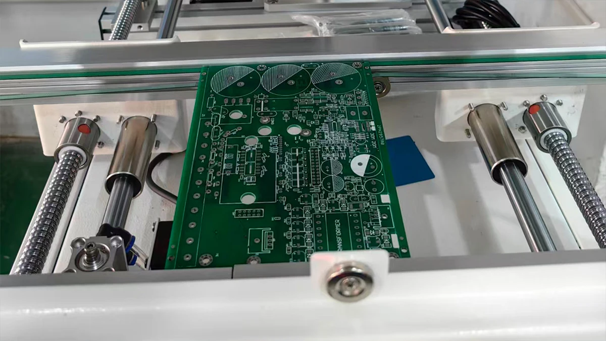
Conditional source screening
Which laser route should you test first?
UV is often a practical first screening route for fine features on selected solder masks, especially where edge control and limited heat-affected change are important. The usable window still depends on the actual formulation, pulse behavior, spot size, focus and scan strategy. Fiber or MOPA at 1064 nm should be treated as a conditional comparison when the mask formulation, pigment or target interaction justifies it. Comparative sample evidence—not mask color alone—should decide the route.
- No wavelength should be approved from mask color alone.
- Average machine power does not define the energy delivered to one feature.
- Spot size, pulse behavior, focus, field position and scan strategy affect the boundary.
- The useful parameter window should tolerate normal material and positioning variation.
| Direction | Why it may be screened | Main boundary | Approval evidence |
|---|---|---|---|
| UV | First-screen fine-feature, color-change or controlled-removal trials when the actual mask absorbs usefully and the optical setup can resolve the required edge. | UV is not automatically “cold”; excessive fluence, poor focus or an unsuitable formulation can still create residue, undercut, breakthrough or poor contrast. | Feature fidelity, contrast/removal, edge condition, layer-below inspection and a repeatable process window across representative boards. |
| Fiber / MOPA | Conditional trials where mask absorption, pigment or the desired interaction supports 1064 nm processing. | May couple strongly to exposed metal or create more heat/contrast variation than desired. | Mask integrity, metal interaction, halo, batch variation and repeatability. |
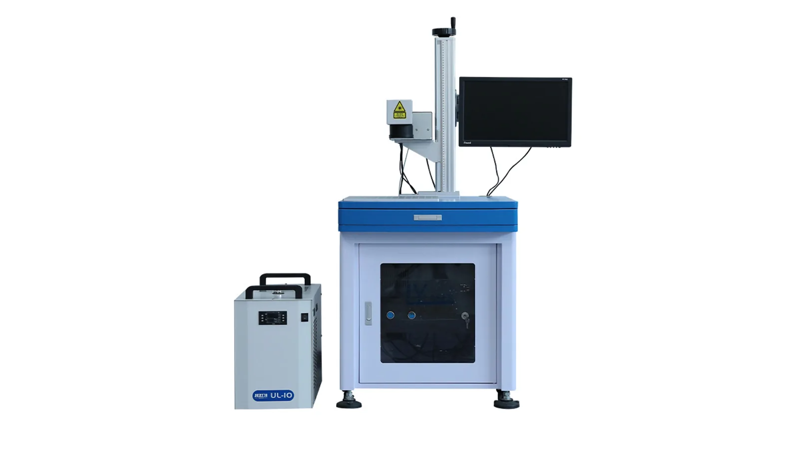
Selection rule: compare source directions on the finished board using the same artwork and inspection method. Approve a stable window, not only the best-looking single setting.
Risks & failure modes
A readable mark can still be outside the safe process window
Define failure limits before testing. Readability alone cannot override solder-mask integrity, conductor protection, acceptable residue or downstream board function.
Approved material result
Artwork, contrast or removal area, edge location and surface condition meet the agreed requirement without unintended layer change.
Readable but not automatically acceptable
Halo, gloss change, roughness, small residue, edge drift or local thinning may require microscopy, cleaning or functional review.
Functional or boundary damage
Unintended copper exposure, conductor attack, mask delamination, insulation loss, laminate damage or a board-function change blocks approval.
From material test to production
When does solder-mask feasibility become a production-system decision?
Once a repeatable, damage-free solder-mask marking window is proven, board support, positioning, verification, loading and cycle requirements become machine-design inputs. The next steps are to validate that window on representative production boards and then translate it into the final machine configuration.
Representative validation
How should a real solder-mask sample be validated?
A single attractive coupon does not prove a production window. Use production-finished boards from the mask, supplier, cure, thickness and surface-finish groups that matter, and inspect the mark again after the downstream processes that the real board will experience.
Freeze the target
Separate color change from ablation. Provide artwork, smallest feature, edge tolerance and the allowed stopping layer.
Group the material
Record mask product, color, supplier, cure, thickness, legend, board finish and batch where available.
Compare a window
Hold the inspection method constant and map stable settings across representative variation, not just one center point.
Recheck after downstream processing
Inspect after the agreed cleaning process and, when relevant to the actual manufacturing route, after reflow or other specified downstream exposure. Recheck contrast or code readability, residue, edge condition, blistering, cracking, lifting and any change in solder-mask integrity.
Translate the approved window to production
Add focus tolerance, field position, fixture repeatability, loading, verification, extraction and cycle targets before selecting the complete machine configuration.
| Record | Minimum detail | Why |
|---|---|---|
| Surface identity | Mask product/color, cure, thickness, legend, board finish and underlying layer | Prevents treating different surface stacks as one material. |
| Target result | Color change or ablation; artwork; smallest feature; mark location | Defines the mechanism and inspection boundary. |
| Visual boundary | Contrast, halo, gloss, roughness, edge drift, residue and cleaning method | Separates readable from cosmetically acceptable. |
| Layer boundary | Allowed copper exposure, stopping layer, undercut and pinhole limit | Protects conductor and insulation requirements. |
| Functional checks | Cleaning result; reflow or other downstream-process check when relevant; electrical, adhesion, environmental or project-specific tests when required | Confirms that a mark which looks acceptable immediately after laser processing remains acceptable in the real board process. |
| Production inputs | Board/panel size, flatness, field, focus variation, fixture, vision, loading, extraction, data/verification and cycle target | Converts the approved material window into the actual machine and workflow requirements. |
Important: a pre-cleaning or pre-reflow pass is not automatically a production pass. If the marked board will be cleaned, reflowed, coated or exposed to another defined downstream process, include that condition in the acceptance plan.
Machine configuration & RFQ
How does the sample result determine the final machine configuration?
The approved material result defines the usable laser route and process margin. The final machine is then sized around feature size, board geometry, positioning tolerance, production volume, verification needs, extraction and safety—not around laser power alone.
Laser source and process window
Select the source family from comparative board tests, then confirm a stable operating window across representative mask and board variation rather than copying one visually attractive setting.
Lens, field and focus strategy
Small modules and fine strokes increase the importance of spot size, field choice and focus stability. Large panels, multiple mark locations or warped boards may require indexing, Z adjustment or additional focus management.
Fixture, positioning and vision
Choose support and locating features around the real board format. If mark position must follow fiducials, board variation or multiple locations, evaluate vision correction instead of assuming the fixture alone can hold the required tolerance.
Extraction, verification and cycle
Plume capture, filtration, cleaning access, reader/verifier requirements, loading method and the complete production cycle can change the final enclosure and automation scope after material feasibility is proven.
Material and marking inputs
- Production-finished PCB or PCBA samples
- Solder-mask product/family, color, cure and thickness if available
- Legend/silkscreen details when the mark overlaps it
- Underlying copper / finish / laminate at the mark location
- Artwork, code type, smallest feature and mark position
- Target result and allowed copper-exposure / damage limits
Production and acceptance inputs
- Board or panel dimensions, flatness/warpage and loading format
- Required throughput or complete cycle target
- Fixture, fiducial, vision or position-correction needs
- Reader/verifier and data-binding requirements if applicable
- Cleaning, reflow or other downstream acceptance checks
- Enclosure, extraction and line-integration constraints
Frequently asked questions
Solder mask laser marking FAQs
Can a laser mark solder mask without exposing copper?
It can be evaluated, but the answer is sample-dependent. Define the required contrast and inspect the actual board for mask thinning, pinholes, edge drift and unintended copper exposure. A readable mark alone is not approval.
Is UV always the best source for solder mask?
No. UV is a common first screening direction for fine marks on selected masks, but the usable process depends on formulation, cure, thickness, underlying finish, optics and the target result. Comparative sample evidence should decide.
Can one setting be reused across PCB suppliers?
Not automatically. Mask formulation, pigment, cure, thickness, legend and surface finish can change. Use a controlled requalification plan when a material, supplier or board stack changes.
What is the difference between color change and ablation?
Color change aims to create optical contrast while keeping the mask functionally intact. Ablation intentionally removes mask to a defined area or stopping layer. Their acceptance criteria and failure risks are different.
Is solder mask the same as silkscreen or legend ink?
No. Solder mask is the functional protective coating over the PCB surface, while legend / silkscreen ink is a separate printed marking layer that is commonly placed on top of the cured solder mask. If laser artwork crosses both, record and validate the two surface conditions separately.
What should I send for a sample test?
Send production-finished boards, solder-mask and board-stack information, legend details when relevant, artwork, smallest feature, target result, mark location, copper-exposure limit, cleaning and downstream-process conditions, acceptance checks, batch variation, board dimensions and production context.
Next step
Send the finished board, the target mark and the acceptance limits
Provide production-finished samples, solder-mask identity and color, cure/thickness information when available, any legend layer at the mark location, the underlying stack, artwork, smallest feature, target result, allowed exposure or damage, downstream-process checks, board dimensions, positioning requirements and cycle target. Zhuorui Laser can then plan a sample comparison and translate the approved window into the machine configuration for quotation.
Request a QuoteOEM & Custom InquiryContact Us