
Applications · Electronics & Electrical
Electronic Component Laser Marking
Small-character identification and traceability for IC packages, capacitors, relays and other electronic components. This page helps you decide which components are marked, what content goes on the part, where the mark can go, how small it can realistically be, and which laser direction to evaluate first.
- Part numbers, 2D codes and polarity marks on ICs, capacitors and relays
- Position discipline across molded epoxy, ceramic and metal-shell surfaces
- UV / fiber / MOPA directions evaluated first, confirmed by sample testing
Quick Answer: Electronic Component Laser Marking at a Glance
Laser marking is widely used for permanent identification and traceability on electronic components, but the useful engineering question is not simply whether a component can be marked. You need to define the actual package and outer surface, the information to be marked, the required visual or code result, the available marking zone, the way the part is presented, the production rate and the downstream processes the mark must survive.
This page helps you turn an initial request such as “mark a code on an IC, capacitor, relay or sensor” into a testable application: identify the component and marking surface, define the target result, choose the first laser route to evaluate, anticipate failure modes, establish sample-acceptance criteria, and use the test results to determine the final optics, fixture, positioning, feeding, verification and machine configuration.
Scope note: this page covers marking the electronic component itself. Board-level marking on PCBs and PCBA is covered by the PCB and PCBA marking page, and connector / terminal marking by the connector and terminal marking page.
Which Electronic Components Are Commonly Laser Marked?
Start with the actual component and the outer layer the laser will reach. Two parts in the same electronics category can require different laser routes because their package surfaces, dimensions and internal structures are different.
IC and chip packages — molded epoxy bodies
ICs, microcontrollers, logic devices and many discrete semiconductor packages use molded epoxy compounds in formats such as QFN, BGA, SOP and similar packages. The usual marking target is the molded top surface. The process has to create readable contrast while keeping thermal and penetration effects within an acceptable window for the real package thickness and internal structure. Deeper material behaviour can be cross-checked against the plastics material pages.
Ceramic components and packages
Ceramic capacitors, resonators, sensors and ceramic-substrate packages may require dark or high-contrast identification on a ceramic surface. Composition, glaze, metallization, thickness and edge sensitivity can change the workable process window, so thin or brittle parts should be evaluated for both readability and surface integrity. See the ceramic substrate material page when the surface response itself is the main unknown.
Metal-shell or plated-surface components
Metal-can crystals, shielded components and other parts with an exposed or intentionally markable metal surface may follow a metal-marking route. The important distinction is the actual outer marking layer: raw metal, anodized metal, plating, coating or an insulating sleeve can require different evaluation. Plated finishes can be reviewed further on the plated metal material page.
Plastic-housed components
Relays, switches, sockets, sensors and other electronic parts may use engineering-plastic housings. Polymer family, colour, fillers, flame-retardant formulation and surface finish can all change contrast and heat response, so the housing material should be confirmed rather than treated as a generic “plastic”.
Why Are Electronic Components Marked?
The mark is usually part of product identification, assembly control or traceability — not decoration.
- Product identification — distinguish part number, model, value, grade or manufacturer information so operators and customers can identify the component correctly.
- Lot and production traceability — connect date, batch, lot or serial data to manufacturing, test and quality records.
- Assembly control — show pin 1, polarity, orientation or other functional cues that help prevent incorrect placement or assembly.
- Quality and recall handling — preserve enough identity to trace affected lots or units when a quality problem has to be investigated.
- Automated verification — provide text or machine-readable codes that can be checked by a camera or reader and linked to MES or other production data where the project requires it.
- Customer or program requirements — apply customer-specific identifiers, UID structures or code content when these are defined by the purchasing or quality specification.
The required reason determines the acceptance method. A polarity dot mainly needs clear, repeatable visibility; a traceability code may also need scanner verification, data matching and a defined reject flow.
What Is Typically Marked on an Electronic Component?
Define the content before choosing the marking field, optics or feeding method, because text density and code size affect the usable process window.
Product identification
Common content includes part numbers, model or value information, manufacturer logos, date codes and lot or batch codes. These marks are usually intended for direct human recognition and should remain legible at the actual viewing distance and component size.
2D codes and serialized traceability
QR codes and Data Matrix symbols can carry serialized or production-linked data such as work order, serial number, lot, test reference or customer part number. On small components, the useful code is not the smallest pattern a laser can draw; it is the smallest pattern that can be produced consistently and read by the specified verification equipment.
Orientation and polarity marks
Pin 1 indicators, polarity marks, dots, lines and other placement cues can be functionally important during SMT or downstream assembly. Their position and contrast therefore need to be treated as acceptance criteria, not just as graphic appearance.
Typical content and data formats
| Mark content | Typical format | Typical purpose |
|---|---|---|
| Part number / model / value | Readable text | Product identification and picking accuracy |
| Date / lot / batch code | Text | Batch traceability and recall handling |
| Serial number | Text / 1D / 2D code | Unit-level identification |
| Traceability code | QR / Data Matrix / GS1 DataMatrix when specified | Link the part to production or customer data |
| Orientation / polarity | Dot, line, symbol or short text | Correct placement and assembly |
| Customer / program identifier | Text or code defined by the customer specification | Program-specific identification and traceability |
What Determines Laser Marking Results on Electronic Components?
The component name alone does not select the process. Mark quality follows from the actual surface, package geometry, feature size, optics, laser parameters and the downstream conditions the mark must tolerate.
| Result variable | What to confirm | Why it changes the result |
|---|---|---|
| Package and outer marking surface | Molded epoxy, ceramic, engineering plastic, coating, plating, sleeve or exposed metal | Different outer layers absorb laser energy differently and produce different contrast, heat and surface-change mechanisms. |
| Surface formulation and condition | Colour, fillers, grade, coating thickness, contamination and supplier / lot variation | Two visually similar parts may require different parameter windows or produce different contrast. |
| Package thickness and internal structure | Thickness at the intended marking zone and proximity of sensitive internal features | Controls how much thermal or penetration margin is acceptable during marking. |
| Mark content and feature size | Character height, stroke width, Data Matrix / QR module size, logo detail | Fine features increase demands on spot size, focus, contrast and scanner capability. |
| Available marking area | Usable zone, edges, leads, terminals, seals and other keep-out boundaries | Constrains code size, layout and the safe location of the mark. |
| Geometry and height variation | Flat, curved, cylindrical, recessed, tray-to-tray height tolerance | Changes focus control, fixture design, rotary needs and whether vision or multi-position handling is required. |
| Laser source, optics and parameter window | Wavelength, pulse behaviour, field lens, working distance, repetition rate, scan speed and passes | The same average power can produce very different thermal load, contrast and feature quality under different combinations. |
| Downstream process | Reflow, washing, coating, handling, thermal cycling and final inspection method | The mark must remain acceptable after the real process sequence, not only immediately after marking. |
Material routing: if the main unknown is how a particular molding compound, ceramic, plastic or plated surface responds to laser energy, use the relevant electronic substrate, plastics or plated metal guidance. The application decision still has to return to the actual component, marking zone, target result and production flow.
How small can the mark realistically be?
Minimum character height, line width and 2D-code module size are configuration-dependent. The practical limit comes from the focused spot, surface contrast, field lens, working distance, part flatness and the scanner or inspection method used at the end. A slightly larger feature that reads consistently across a batch is more useful than the smallest feature achieved on one sample. For deeper optics guidance, see the micro-marking guide.
What Marking Result Should You Target?
Define the pass condition before the sample test. “Looks good” is not enough to choose a repeatable production configuration.
- Visual result — define whether you need light-on-dark, dark-on-light or simply sufficient contrast for reliable human recognition.
- Character and code result — define the target character size, stroke clarity, module size, scanner and any agreed verification or grading method.
- Position result — define the approved marking zone, edge clearance, datum or orientation reference, and the amount of position variation the product can accept.
- Surface / functional result — define what damage is unacceptable, such as cracking, melting, excessive carbonization, coating breakthrough, terminal damage or other visible changes that could affect function or reliability.
- Durability result — define which real downstream processes the mark must survive, such as reflow, washing, coating, handling or thermal cycling.
- Consistency result — define whether the same acceptance window must cover multiple component lots, suppliers, colours or package variants.
- Production result — define the required station throughput, verification timing and reject handling rather than judging laser scan time alone.
These targets become the acceptance criteria used later to compare UV, fiber or MOPA trials and to decide whether optics, fixture, vision, feeding or automation changes are necessary.
How Do Marking Area, Geometry and Part Handling Affect the Result?
Small components leave little room for error. The usable marking zone, part height, orientation and presentation method often determine the fixture and positioning strategy before the laser recipe is finalized.
Prefer a dedicated marking surface with enough clearance from terminals, seals, edges and other functional features. The safe zone has to be defined from the actual package drawing or sample and then verified during testing; it should not be inferred from the component category alone.
Typical marking zones
- Molded package top — common for text and 2D codes on IC packages when the package structure and thickness provide an acceptable process window.
- Ceramic or coated face — usable when terminations, metallized areas and sensitive edges are excluded from the marking zone.
- Plastic housing face — useful on relays, sensors or other housings when the polymer formulation produces a stable mark.
- Cylindrical side surface — may require rotary handling or controlled indexing if the mark extends around the circumference.
Keep-out zones
- Leads, pins, solder terminations and contact areas — avoid damaging plating, solderability or electrical contact surfaces.
- Seals and functional interfaces — do not let the mark breach or weaken hermetic, adhesive or sealing regions.
- Thin edges and mechanically stressed regions — edge-sensitive ceramic or thin packages may require additional clearance and lower thermal loading.
- Unverified internal-risk zones — if package thickness or internal construction is uncertain, confirm the marking zone on drawings or samples rather than assuming an XY position alone eliminates internal risk.
How the part is presented to the laser
A flat part in a repeatable pocket can often use a simple fixture. Randomly oriented parts may need vision positioning. Cylindrical parts may need a rotary axis. Tray, magazine, tape-and-reel or feeder presentation also changes how position repeatability, focus and cycle time have to be validated.
Which Laser Should You Test First for Electronic Component Marking?
UV, fiber and MOPA cover many electronic-component applications, but the first route should follow the actual marking surface and target result, then be confirmed on real parts.
UV (~355 nm) — often a first evaluation for molded compounds, ceramics and fine detail
UV lasers are commonly evaluated first when molded epoxy, selected plastics, ceramics or very fine features require a controlled surface effect with limited thermal loading. The useful window still depends on the actual compound, colour, thickness and target contrast, so “UV” is a starting direction rather than a guaranteed recipe.
Fiber (~1064 nm) — strong candidate for exposed metal and compatible coated surfaces
Fiber lasers are a standard direction for metal marking and can be suitable when the actual target layer is exposed metal, anodized metal or another compatible surface. Molded packages and insulating outer layers require a separate evaluation; do not select fiber simply from the component name when the laser is actually hitting a sleeve, coating or polymer surface.
MOPA fiber — wider pulse-control window for selected surfaces
MOPA is a fiber-laser architecture with a broader pulse-width and frequency adjustment range. It can be useful where contrast and heat balance need more process-window flexibility on selected metals, coatings or compatible compounds, but whether it is better than Q-switched fiber or UV has to be demonstrated on the target surface.
Micro-marking: spot size, field lens and verification limit
A smaller marking field can support finer features, but it reduces usable area and can create a trade-off with tray coverage or multi-part marking. Field lens, working distance, spot size, focus tolerance and scanner capability therefore have to be evaluated together. The correct target is the smallest feature that remains repeatable and verifiable across the required production variation.
Why laser power alone does not determine mark quality
Average power by itself does not define a good component mark. Pulse energy, pulse width, repetition rate, scan speed, spot size, number of passes and the surface response interact. A recipe that builds contrast safely on one compound can overheat another, so the process window should be developed on real samples rather than copied from a catalogue.
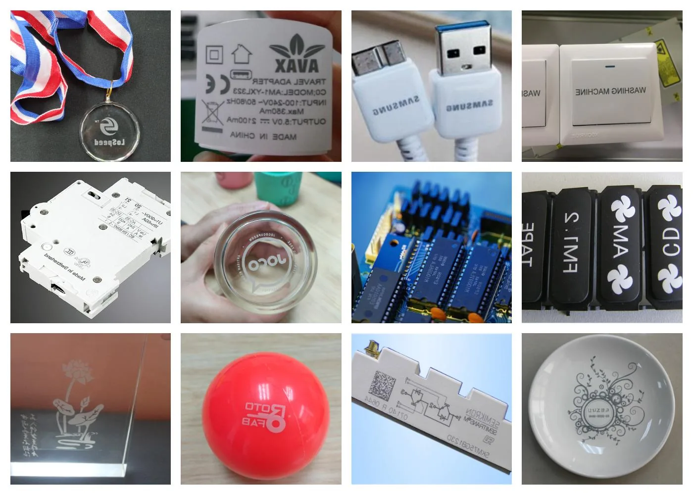
Engineering takeaway: this is a supportive visual, not a verified result for a specific electronic component; the final laser source and parameter window should be confirmed on the actual part.
For equipment families, see the UV laser marking machines and fiber laser marking machines pages after the sample route has been narrowed.
What Are the Common Electronic Component Laser Marking Failure Modes?
Failure modes help you diagnose whether the problem comes from the surface, optics, parameter window, positioning or production data flow.
| Failure mode | What you may see | What to re-check |
|---|---|---|
| Low or inconsistent contrast | Text or code varies in darkness / lightness across parts or lots | Surface formulation, colour, contamination, lot variation and laser parameter window |
| Blurred or filled-in fine features | Small characters merge, thin strokes disappear or code cells lose definition | Spot size, focus, field lens, feature size, scan speed and energy density |
| 2D-code read failure | The pattern is visible but scanner reads are intermittent or grading is poor | Module size, contrast, cell shape, quiet zone, scanner setup and verification method |
| Excessive thermal effect | Melting, carbonization, discoloration, deformation or an enlarged heat-affected area | Laser source, pulse behaviour, accumulated energy, passes and scan strategy |
| Package or ceramic damage | Cracking, chipping or other unacceptable surface / structural change | Part thickness, edge distance, thermal load, focus and marking-zone selection |
| Position drift | Mark moves toward an edge, terminal or keep-out region | Fixture repeatability, tray tolerance, part orientation, datum strategy and vision need |
| Focus variation across parts | Some parts in the tray mark sharply while others lose contrast or definition | Part-height variation, tray flatness, field / focus tolerance and presentation method |
| Wrong content or wrong-part marking | The physical mark is readable but the data does not match the component or production record | Part identification, data source, MES / database handshake, verification and reject logic |
A failed sample does not automatically mean laser marking is unsuitable. The failure should be classified first, then the relevant variable — source, optics, recipe, fixture, positioning, data logic or handling — should be changed deliberately and re-tested.
How Does Electronic Component Marking Fit Into the Production Workflow?
A production cell has to control the entire part-and-data flow, not only the laser scan.
1. Present and identify the part
Components may arrive in trays, magazines, tape-and-reel, feeders or dedicated fixtures. The system has to ensure that the correct part is present, oriented correctly and located within the marking tolerance before the job starts.
2. Load or generate the marking data
Static text can come from the marking job file; variable data may come from a serial-number source, barcode, MES or database. The project should define what identifies the part, which system owns the data and what happens if the required data is missing or invalid.
3. Position, focus and mark
Simple pockets may provide enough repeatability for fixed positioning. Random locations can require vision alignment; moving production lines may use flying / online marking; cylindrical parts may require rotary handling.
4. Verify the mark and the data
Verification can check presence, position, readable text, code readability and — where required — whether the marked value matches the expected production data. The verification point should be chosen deliberately: immediately after marking, after a downstream process, or at final inspection.
5. Handle failures and record the result
A production design should define what happens when verification fails: stop the station, reject the part, divert it, allow controlled rework, or request operator review. If traceability is required, pass / fail status and relevant identifiers may also need to be recorded through the traceability integration layer.
6. Match handling method to volume
Tray and magazine handling suit many batch or changeover-heavy applications. Tape-and-reel and feeder-based presentation can support higher-volume SMD flow. The real cycle time includes loading, locating, data handling, marking, verification, reject handling and unloading — not just scan time.
7. Include extraction, enclosure and laser safety in the cell design
Marking molded compounds, plastics or coatings can generate fumes or particulate, so extraction requirements should be evaluated for the actual material and process. UV and 1064 nm laser radiation are invisible, and the laser safety classification belongs to the complete system; an enclosed-looking machine should not be assumed to be Class 1 without system-level assessment.
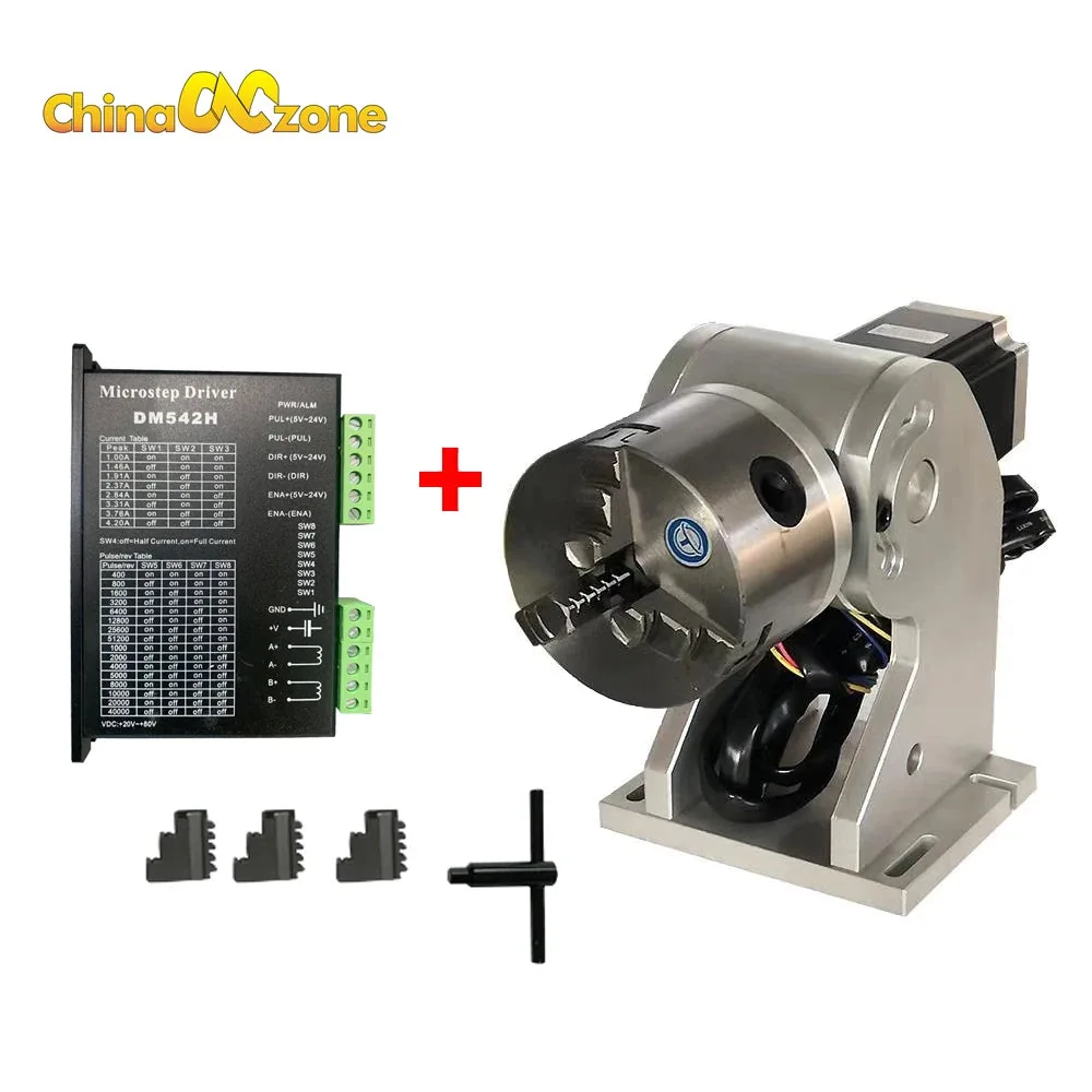
Engineering takeaway: the accessory illustrates rotary workpiece handling; actual compatibility, component size and production setup must be confirmed for the project.
How Should a Sample Marking Test Be Accepted?
Agree the pass / fail criteria before comparing samples, so the selected process is based on the result your production actually needs.
| Acceptance item | What to verify |
|---|---|
| Correct content | The text, serial value, lot information or 2D-code data matches the approved input. |
| Marking position | The mark stays inside the approved marking area and away from defined keep-out regions. |
| Visual quality | Contrast, character edges and feature consistency meet the agreed visual requirement across the sample set. |
| Code readability | The specified reader can read the code reliably; if a grading requirement applies, use the agreed verification method and target rather than visual judgement alone. |
| Surface and package condition | No unacceptable cracking, melting, carbonization, coating damage, terminal damage or other defined surface / functional defect is present. |
| Downstream durability | Re-check the mark after the actual reflow, washing, coating, handling or thermal process that applies to the product. |
| Lot / supplier consistency | Where multiple compound lots, colours, finishes or suppliers are used, confirm that the accepted process window covers the required variation. |
| Production repeatability | Confirm position, readability and quality across the intended fixture / tray / feeder method and at the required station cycle. |
If your project uses code grading — for example ISO/IEC 15415, or ISO/IEC 29158 where direct-part-mark verification is applicable — agree the standard, verifier setup and acceptance target with the quality team before the sample run. A standard describes how the result is evaluated; it does not guarantee that one parameter set will meet the same grade on every surface.
The sample marking test checklist can be used to prepare the components and acceptance information before evaluation.
How Do Sample-Test Results Determine the Final Machine Configuration?
The final machine should be the consequence of the accepted sample and production findings — not a model selected before the process window is understood.
| What the test or production review shows | What it changes in the configuration |
|---|---|
| UV gives the required contrast and feature quality with an acceptable surface condition | UV remains the candidate source family; the next step is to lock the required power class, optics and working field from the accepted recipe and throughput. |
| An exposed metal or compatible coated surface gives the required result with fiber | Fiber becomes the candidate source route; lens, field and pulse / power class are then matched to the accepted result and cycle requirement. |
| A wider pulse-control window materially improves contrast or heat balance | Evaluate a MOPA fiber configuration rather than treating all fiber sources as interchangeable. |
| Fine characters or code modules are not repeatable over the required large field | Re-evaluate field lens, working area, spot size and whether the tray / workpiece should be indexed through multiple positions. |
| Position variation causes marks to drift toward keep-out zones | Improve the fixture / datum strategy or add vision positioning when mechanical repeatability alone is insufficient. |
| Part height variation moves some components out of focus | Improve presentation flatness, fixture height control or use a configuration that can accommodate the required focus variation. |
| The mark must wrap around a cylindrical surface | Add an appropriate rotary or indexed handling configuration and confirm the usable diameter / length range. |
| Manual loading cannot meet the required station throughput | Move from a simple workstation toward tray indexing, tape-and-reel, feeder or project-based automation. |
| Verification and data matching are mandatory | Add the required camera / reader, data interface, result logging and reject logic to the cell definition. |
| Material processing creates unacceptable fume or operator-exposure risk | Specify extraction, enclosure, interlocks and the appropriate system-level laser-safety architecture. |
Information to send with samples or an RFQ
- Component type, package, dimensions and photos or drawings of the intended marking zone
- Actual outer surface / finish and any known material or supplier variations
- Mark content, code format, target character or module size and required marking position
- Keep-out zones and any functional / cosmetic damage limits
- Feeding method: tray, magazine, tape-and-reel, feeder, rotary or other presentation
- Required throughput, verification timing and reject-handling requirement
- MES / database / data-interface requirements where variable traceability is needed
- Downstream processes and the sample-acceptance criteria the mark must pass
The RFQ checklist resource can be used to package these inputs for a standard-machine quotation or a project-based configuration review.
FAQ
Can a laser mark the molded epoxy body of an IC without damaging the package?
Molded IC bodies are commonly laser marked, but a safe result depends on the molding compound, package thickness, internal construction, marking zone and laser parameter window. The correct route is to define the acceptable visual result and damage limits, then confirm them on real samples rather than assume that package type alone guarantees the result.
What is the smallest character or 2D code that can be marked on a small component?
The minimum useful feature size depends on spot size, optics, focus tolerance, surface contrast and the reader or verification method. The practical limit is the smallest feature that remains repeatable and readable across the required sample and production variation.
Why is UV often evaluated first for IC and ceramic component marking?
UV is often a strong first candidate when fine features and controlled thermal loading are priorities on selected molding compounds, plastics or ceramics. Actual absorption and surface response vary by formulation and construction, so the final route still has to be confirmed on the target component.
Can fiber or MOPA be used on capacitor or metal-can components?
They can be strong candidates when the actual outer marking layer is compatible with fiber marking, especially exposed metals and selected coated surfaces. Confirm what the laser is physically hitting — metal, coating, plating, plastic or sleeve — before selecting the source from the component name alone.
Does component laser marking survive reflow, washing and thermal cycling?
It can, but durability depends on the actual surface, mark mechanism and downstream conditions. If reflow, washing, coating or thermal cycling matters to your product, include those steps in the sample-acceptance sequence and re-check readability and surface condition afterwards.
Can the process be integrated with tape-and-reel, vision or rotary handling?
Yes, these are common configuration directions when the component form and production flow require them. The final choice depends on part presentation, orientation tolerance, required throughput, verification and the accepted sample process window.
Ready to Evaluate Electronic Component Marking for Your Production?
Send your component type, surface material, mark content and target character or code size, and we will review the application, confirm the laser direction and prepare a sample marking test.